
Page 70
conferenceseries
.com
Volume 7
Innovative Energy & Research
ISSN: 2576-1463
Advanced Energy Materials 2018
August 13-14, 2018
August 13-14, 2018 | Dublin, Ireland
20
th
International Conference on
Advanced Energy Materials and Research
Graphene-silicon Schottky heterojunctions for optoelectronic applications
Antonio Di Bartolomeo
1
, Giuseppe Luongo
1
, Laura Iemmo
1
, Francesca Urban
1
and
Filippo Giubileo
2
1
Università di Salerno, Italy
2
CNR-SPIN, Italy
T
he graphene/silicon (Gr/Si) junction has been the subject of an intense research activity both for the easy fabrication and
for the variety of phenomena that it allows studying. It offers the opportunity to investigate new fundamental physics at
the interface between a 2D semimetal and a 3D semiconductor, and holds promises for a new generation of graphene-based
devices such as photodetectors, solar cells and chemical-biological sensors. A Gr/Si junction with defect-free interface exhibits
rectifying current-voltage (I-V) characteristics, which are the result of the formation of a Schottky barrier, as in traditional
metal-semiconductor (M/S) Schottky diodes. The vanishing density of states at the graphene Dirac point enables Fermi level
tuning and hence Schottky barrier height modulation by a single anode-cathode bias. When the Gr/Si junction is used as a
photodiode, graphene acts not only as anti-reflecting and transparent conductive layer for charge transport to the external
circuit, but it functions also as active material for light absorption and electron-hole generation and separation. Although
most of the incident light is converted to photocharge into Si, the absorbance in graphene enables detection of photons with
Si sub-bandgap energy through internal photoemission over the Schottky barrier. Photo charges injected over the Schottky
barrier, under high reverse bias, can be accelerated by the electric field in the depletion region of the diode and cause avalanche
multiplication by scattering with the Si lattice, thus enabling internal gain. The Gr/Si junction forms the ultimate ultra-shallow
junction, which is ideal to detect light absorbed very close to the Si surface, such as near- and mid-ultraviolet. In this talk,
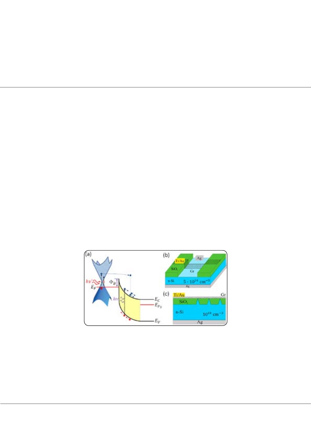
we present the electrical characterization and the photoresponse of two types of Gr/Si devices, shown in figures 1 (b) and
(c). Although due to different mechanisms, on both devices we demonstrate photo-responsivity exceeding 2.5 A/W that is
competitive with present solid-state devices. We attribute it to the contribution of charges photogenerated in the surrounding
region of the flat junction or to the internal gain by impact ionization caused by the enhanced field on the nano tips.
Figure 1: (a)
Photodetection in a Gr/Si junction. Photons with energy lower than the Si bandgap, E
G
= E
C
– E
v
but higher than the Schottky barrier
Φ
E
(
Φ
B
<
hv < E
G
) can be absorbed in graphene. Emitted over the Schottky barrier, such electrons can originate avalanche multiplication through impact ionization. (b)
Graphene on flat Si substrate (“flat Gr/Si” junction) and (c) graphene on patterned Si (Gr/Si-tips junction)
Recent Publications:
1. Di Bartolomeo A (2016) Graphene Schottky diodes: An experimental review of the rectifying graphene/semiconductor
heterojunction. Physics Reports 606:1-58.
Antonio Di Bartolomeo et al., Innov Ener Res 2018, Volume 7
DOI: 10.4172/2576-1463-C1-002


