Our Group organises 3000+ Global Conferenceseries Events every year across USA, Europe & Asia with support from 1000 more scientific Societies and Publishes 700+ Open Access Journals which contains over 50000 eminent personalities, reputed scientists as editorial board members.
Open Access Journals gaining more Readers and Citations
700 Journals and 15,000,000 Readers Each Journal is getting 25,000+ Readers
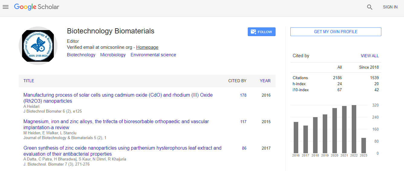
Google Scholar citation report
Citations : 3330
Journal of Biotechnology & Biomaterials received 3330 citations as per Google Scholar report
Indexed In
- Index Copernicus
- Google Scholar
- Sherpa Romeo
- Open J Gate
- Genamics JournalSeek
- Academic Keys
- ResearchBible
- China National Knowledge Infrastructure (CNKI)
- Access to Global Online Research in Agriculture (AGORA)
- Electronic Journals Library
- RefSeek
- Hamdard University
- EBSCO A-Z
- OCLC- WorldCat
- SWB online catalog
- Virtual Library of Biology (vifabio)
- Publons
- Geneva Foundation for Medical Education and Research
- Euro Pub
- ICMJE
Useful Links
Recommended Journals
Related Subjects
Share This Page
Designing smart carriers for biosensors, tissue engineering, and directed cell growth by teaming up semiconductor wafers from micro/nano-electronics and polymer supports from biotechnology
World Bio Summit & Expo
Heidemarie Schmidt
TU Chemnitz, Germany
ScientificTracks Abstracts: J Biotechnol Biomater
Abstract
State-of-the-art carriers for biosensors, tissue engineering, and directed cell growth are chemically functionalized and coated by polymers to operate under physiological conditions. There is still a strong demand for the development of smart carriers with high accuracy, selectivity, lower detection limits and robustness during autoclaving for sterilization, incubation for cell growth, and cryogenic applications for shock freezing. We have implanted ions in ca. 200 - 1000 nm thick layers of semiconductor wafers, in order to realize defined microscopic to nanoscopic patterns of surface-near electrostatic forces (SNEF). Finally, these charge patterned silicon wafers are protected by a thin 2-3 nm thick insulting oxide layer. The estimated density of localized charges between the native silicon dioxide and the silicon carrier ranges from 1014 to 1018 m-2 and is much larger and stable than charges from silanol groups at an ordinary silicon dioxide surface. Using combined Atomic and Kelvin probe force microscopy measurements (KPFM), we could prove that positively and negatively charged polymers are preferentially adsorbed at n-type and p-type conducting regions of the of locally implanted silicon carrier with different SNEF patterns. Moreover from KPFM measurements, we know that the SNEF can be minimized by applying an appropriate bias to correspondingly structured back electrodes.Biography
Heidemarie Schmidt has completed her PhD at the University Leipzig. Since 2003, she and her team from the “Nano-Spintronics” group has been developing new materials for neuromorphic computing, transparent spintronics, magnetooptics, and for smart carriers in biotechnology at the University Leipzig, HZDR, and TU Chemnitz. She has published more than 150 papers in reputed journals and serves as an advisory program committee member for the international workshop in Ellipsometry WSE-2014 and WSE-2015. She received the Nano-Future prize from the Bundesministerium für Bildung und Forschung (2002) and a Heisenberg Fellowship from the German Science foundation (2011).

 Spanish
  Chinese
  Russian
  German
  French
  Japanese
  Portuguese
  Hindi
Hindi 
