Research Article Open Access
Performance Analysis of Graded p-i-n Junction Solar Cell by using Suitable Materials
Md. Toufique Arefin* and Afsana NadiaDept. Of EEE, East West University, Jahurul Islam City, Aftabnagar, Dhaka, Bangladesh.
- *Corresponding Author:
- Md. Toufique Arefin
Dept. Of EEE, East West University, Jahurul Islam City, Aftabnagar, Dhaka, Bangladesh
E-mail: toufique88@gmail.com
Visit for more related articles at International Journal of Advance Innovations, Thoughts & Ideas
Abstract
Documentation related which identifies the documentations that represent the same real-world entity, is an important step for data integration. A discovery shopping search engine tool is designed in order to remove the reproductions of documentation obtained from the query outcomes of numerous web databases and as well as to help shoppers make ideal buying decisions. To address the problem of documentation related in the web database scenario, we present an unsupervised, online documentation related method UDD which, for a given query can effectively identify reproductions from the query outcome documentations of numerous web databases. Most of the documentation related methods are supervised, which requires the client to provide training data. These methods are not applicable for the web database scenario. Hence an unsupervised and on-line approach with client perspective based search is offered for search within search.
Keywords
Solar cell, GaInAsP, band gap, efficiency.
Introduction
A solar cell is formed by a light sensitive p-n junction semiconductor where the photons of the sunlight are absorbed. Every photon has its own energy. If the energy of the photon is greater than or equal to the energy needed to transfer electron from the valance band to the conduction band, it will contribute to the output of the solar cell. The probability of releasing electrons by the photons depends on the amount of light absorbed by the cell’s surface. More absorption implies more electron release, and hence more electricity will generate (Palaniappan, Phillip & Nandagopal, 2000). We can model an equivalent circuit which will help to understand the electronic behavior of a solar cell. Figure 1 shows the equivalent circuit diagram of a solar cell. An ideal solar cell may be represented by a current source in parallel with a diode (Kumar & Saraswathi, 2001). But in practical case no solar cell is ideal.

Figure 1: The Equivalent Circuit of a Solar Cell.
Solar cells are used for converting the photon energy to electrical energy. When sunlight falls on the solar cell, the materials absorb the photons (if the photon’s energy is equal or greater than the energy gap of that material) and produce electricity. In 1839, the French physicist Antoine-César Becquerel started the work for developing the solar cells (Goetzberger & Hoffmann, 2005). By experimenting with a solid electrode in an electrolyte solution, he observed that when light fell upon the electrode, the voltage developed in electrode. After a long period (around 50 years) the first true solar cells were constructed by Charles Fritts using junctions formed which were coated by the semiconductor selenium with an ultrathin, which is nearly transparent, layer of gold. But the devices were very inefficient for use, because it could transform the absorbed light’s energy to electrical energy and the efficiency was less than 1 percent of the absorbed light. In 1927, for the solution of that problem, other metal semiconductor-junction solar cells were discovered which was made of copper and the semiconductor copper oxide. In 1930s in the fields of light-sensitive devices, both the selenium cell and the copper oxide cell were being employed, such as photometers, for use in photography. The early solar cell had energy-conversion efficiency less than 1 percent. In 1941, this problem was finally overcome with the development of the silicon solar cell by authors (Ohl, Silver & N.J., 1941). A silicon solar cell was invented in 1954 by three American researchers G.L. Pearson, Daryl Chapin, and Calvin Fuller, which had 6-percent energy-conversion efficiency using direct sunlight’s photons (Pahuja, 2005). By the late 1980s not only silicon cells but also those made of Gallium Arsenide which was capable of more than 20 percent efficiency had been fabricated. After that a concentrator solar cell is invented in1989.
In our project, we are interested to design a graded p-i-n junction solar cell to improve efficiency by causing absorption of wider spectrum of sunlight. There are mainly two ways to grade a junction. One is putting an impurity that means doping the materials and another is by changing the compositions of the materials. Here we have used quaternary semiconductor material, GaInAsP because it is easy to change the band gap of this material without changing the lattice constant and we can also change the band gap over a wide region by changing their composition. Finally we have modeled our solar cell.
The rest of this paper is organized as follows. Section 2 introduces the properties of compound semiconductor materials. In section 3, material properties are analyzed (such as, energy gap analysis and lattice parameter analysis etc). In section 4, we have modeled our desired p-i-n solar cell. Finally, section 5 gives conclusions for the paper.
Properties of Compound Semiconductor Materials
In this section, we have discussed about different types of binary semiconductor materials that form GaInAsP quaternary materials and energy gap relationships.
Quaternary GaInAsP Materials on InP Substrate
We have to consider two cases before choosing our substrate materials. One of the important cases is that the substrate material should be cost effective, because substrate material is not the main part of the cells (because it’s not absorbing the photon energy). Generally researchers choose substrate materials, which should be cost effective. Binary materials are also used as substrate, because those semiconductors are also cost effective. The most important case is that the lattice constant of the substrate should be matched with the active semiconductor materials (but a little mismatch is acceptable). Here active semiconductor material means which part of the solar cell is associated with absorbing photon’s energy. For our project, we choose substrate as InP and active semiconductor material as GaInAsP. We choose InP because its lattice constant is pretty close with GaInAsP. The lattice constant of InP is 5.8687 A. Lattice constant of Ga0.47In0.53AsyP1-y is 5.8687 A at 300K. So for this composition, we can see that the lattice constant is identical with InP. Because of that we use Quaternary GaInAsP materials on InP substrate.
Why Choose this Material
In our project, we have used quaternary semiconductor material which is GaInAsP. Because we can easily control the lattice parameter and band gap of this material. If we vary the composition then we can get band gap and lattice constant as a range. For GaxIn1-xAsyP1-y , where the compositions are x and y which are also called mole fractions. Now if we vary composition of x and y, then the range for band gap is 2.073-0.5153 eV. This means that our solar cell can absorb a large portion of sunlight’s spectrum. This is much desired case for our project, because if we could absorb large portion of sunlight’s spectrum that means the efficiency of our solar cell will increase. But we cannot take above bang gap range, because for that composition that we have got the range, the lattice parameter of GaInAsP could be mismatched with the substrate InP.
Energy Gap Relationships
In this section, we present the relationship to calculate the band gap of GaInAsP. For that purpose, first we have to know for which composition, we want to calculate the band gap. Now the formula for finding the band gap of quaternary materials in terms of the band gaps of ternary semiconductor materials is given below (Piprek, 2005),
 ( 1)
( 1)
Let's assume that, 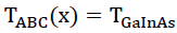 The formula for finding the band gap of ternary materials in terms of the
band gaps of binary semiconductor materials is given below (Piprek, 2005),
The formula for finding the band gap of ternary materials in terms of the
band gaps of binary semiconductor materials is given below (Piprek, 2005),
 (2 )
(2 )
Where, ‘CABC’ is an empirical bowing parameter. According to Vegard’s law, CABC = 0 for the lattice constant. However, strong bowing is often observed for energy gap. Experimentally, bowing parameters determined the direct band gap. Now we want to calculate,
Now, 
Another formula for finding the band gap of quaternary material is (Levinstein, Rumyantsev & Shur, 1999),
 (3)
(3)
Lattice Parameter Relationships
When we model any solar cell then we have to consider one important issue and that is lattice constant mismatch. The lattice constant of our quaternary semiconductor material (GaInAsP) should be matched with the substrate material (InP). If the lattice constant is not matched then the whole property that we consider could be changed. The formula of lattice constant of quaternary semiconductor is given below (Moon, Antypas & james, 1974),
Lattice constant = 5.87+0.18x-0.42y+0.02xy Ǻ (4).
Analysis of Material Properties
In this section, material properties are analyzed. At first, energy gap analysis and Lattice parameter analysis has given below. Then simulation has been done for that analysis.
Energy Gap Analysis
Now if we vary the composition of x and y from 0 to 1 respectively of GaInAsP, then we get a surface, where the maximum energy gap is 2.0731 eV and minimum band gap is 0.5135 eV.
Figure 2 is about the band gap vs. composition and from MATLAB plot we can see the maximum, minimum band gap and as well as their corresponding composition too. The lattice constant at maximum and minimum band gap are respectively 5.6620 A and 5.4540 A.

Figure 2: Band Gap vs. Composition
Lattice Parameter Analysis and Simulation
Now if we vary the composition, then we get a surface for lattice constant and the maximum and minimum lattice constant are 6.042 A and 5.452 A. Figure 3 shows the surface for lattice constant while we varying the composition. From figure, we can see that the range of lattice constant is from 6.042 A and 5.452 A.

Figure 3: Lattice Constant vs. Composition.
Lattice Constant under Certain Condition
Here we consider that ±0.05% lattice constant mismatch with InP is acceptable. Now the surface for required lattice constant is showed in figure 4.

Figure 4: Required Lattice Constant vs. Composition.
Analysis under Restricted Lattice Constant
Under ± 0.05% lattice constant mismatch, the maximum and minimum lattice constants are 5.8980A and 5.8394A and the corresponding compositions are x=0.3800, y=1 and x=0.2400, y=0.3800 respectively. Again at maximum and minimum lattice constant the corresponding energy gaps are 0.5135 eV and 1.2013eV respectively. Now maximum and minimum band gaps are 1.3763 eV and 0.5135 eV. At maximum band gap, lattice constant and composition are respectively 5.8658A and x=0.0100, y=0. At minimum band gap, lattice constant and composition are respectively 5.8980A and x=0.3800, y=1. These restricted values of the compositions and band gaps will be used to design the graded p-i-n solar cell.
Modeling p-i-n Solar Cell
In this section, we first model our desired p-i-n solar cell first. For this purpose, we have to find out the penetration depth for 901 and 2416 nm wave length. We put at the top the material for which we can get higher band gap, because the penetration depth for high frequency is low and for low frequency the penetration depth is high. So we put at the bottom the material for which the band gap is lower. Here, some required values:
1. Maximum band gap =1.3763 eV and the corresponding wave length is 901 nm.
2. Minimum band gap = 0.5135 eV and the corresponding wave length is 2416 nm.
So our solar cell can absorb those photons which have the wave length between 901 nm-2416 nm. Figure 5 shows the solar spectrum and the bounded region shows the area that our solar cell can absorb.

Figure 5: Solar Spectrum and the Absorbed Wavelength in nm.
Now we want to calculate the percentage of solar spectrum that our solar cell could absorb.
The total energy of solar spectrum=1.0004e+003 (W/m2)
The absorbed energy = 306.5067 (W/m2)
Percentage =30.639%
So, our solar cell can absorb 30.6393% of solar radiation. Now we want to calculate the penetration depth for those photons which have energy of 1.3763 eV and 0.5135 eV respectively. For this calculation, we have used MATLAB software and the MATLAB plot for this calculation is shown in figure 6 and figure 7 respectively

Figure 6: Penetration Depth vs. Photon Energy for 1.37 eV.

Figure 7: Penetration Depth vs. Photon Energy for 0.5135 eV.
Figure 6 shows the penetration depth for the photon which has an energy around 1.37 eV and from the plot we can see that the penetration depth for that energized photon is around 2.108 10-07 m that mean around 0.2108 um.
Figure 7 shows the penetration depth for the photon which has an energy around 0.5135 eV and from the plot we can see that the penetration depth for that energized photon is around 9.753 10-06 m that mean around 10 um. We also calculate the penetration depth for those photons which have a wave length of 901 nm and 2416 nm respectively. Now we can model our p-i-n solar cell, because we got every parameter to design our desire solar cell. Figure 8 shows our modeled p-i-n solar cell. For the composition we get the band gap 1.3723 eV that we have to put on the top of the p-i-n solar cell, because the high frequency photon’s penetration depth is low. Then we put an intrinsic material between p and n type doped material (here we use intrinsic material as GaxIn1-xAs1-yPy and which is not doped at all). Finally at the bottom we put n-type material.

Figure 8: Modeled p-i-n Solar Cell.
Conclusion
A simple p-i-n solar cell model is developed by using GaInAsP semiconductor material. For this purpose we choose GaInAsP as active semiconductor material of solar cell and InP as substrate, because its lattice constant are pretty close with GaInAsP. We have analyzed energy gap and lattice parameter of GaInAsP. From the analysis, it is cleared that our p-i-n solar cell would cover wider spectrum of sunlight without effective change in the lattice constant. In our paper, we have used ±0.05% mismatch in lattice parameter to cover wider range from sunlight spectrum but in future this mismatch can be increased to cover wider range. In future, dark current, short circuit current and net current but fill factor, open circuit voltage and efficiency would be calculated for better performance. We have used GaInAsP to design our p-i-n solar cell but in future other quaternary materials can be used. The work is under investigation and will be reported soon.
Acknowledgements
The authors would like to acknowledge with thanks the Dr. Anisul Haque, Professor, Department of Electrical and Electronic Engineering (EEE), East West University (EWU), Dhaka, Bangladesh for his valuable discussions, suggestions and constant support in the preparation of this paper..
References
- Harish Palaniappan, Kathy L. Phillip and Preethsa Nandagopal. Solar Cells. 2000.
- I. Ravi Kumar and N. Bala Saraswathi. Principal of Optical Communication and Opto Electronics. Laxmi Publications, New Delhi, 2001.
- A Goetzberger and V.U.Hoffmann. Photovoltaic Solar Energy Generation. Springer-Varlag Berlin Heidelberg, Germany, 2005.
- Russell S. Ohl, Little Silver and N.J. Light-sensetive electronic device. U.S. Patent 2,402,662 , New York, 1941.
- Om Prakash Pahuja. Solid State Physics. Laxmi Publications LTD, New Delhi, 2005.
- Joachim Piprek. Semiconductor Optoelectronic Devices: Introduction to Physics and Simulation. Springer Science+Business Media Inc., New York, USA, 2005.
- M. Levinstein, S. Rumyantsev and M. Shur. Handbook Series on Semiconductor Parameters. vol. 1,2, World Scientific, London, 1999.
- R.L.Moon, G.A.Antypas and L.W. James, Bandgap and lattice constant of GaInAsP as a function of alloy composition. Varrian labrotaries, Palo Alto, California, pages 635, 1974.
Relevant Topics
- Advance Techniques in cancer treatments
- Advanced Techniques in Rehabilitation
- Artificial Intelligence
- Blockchain Technology
- Diabetes care
- Digital Transformation
- Innovations & Tends in Pharma
- Innovations in Diagnosis & Treatment
- Innovations in Immunology
- Innovations in Neuroscience
- Innovations in ophthalmology
- Life Science and Brain research
- Machine Learning
- New inventions & Patents
- Quantum Computing
Recommended Journals
Article Tools
Article Usage
- Total views: 14931
- [From(publication date):
May-2013 - Apr 04, 2025] - Breakdown by view type
- HTML page views : 10318
- PDF downloads : 4613