Research Article Open Access
Optical and Electrical Si-Based Biosensors: Fabrication and Trasduction Issues
Libertino S1*, Conoci S2, Santangelo MF1, Pagano R1, Sciuto EL3, Sinatra F3, Sanfilippo D2, Fallica G2 and Lombardo S1
1CNR - IMM, VIII strada Z.I., 5, Catania, Italy
2STMicroelectronics, Stradale Primosole 50, Catania, Italy
3University of Catania – G.F. Ingrassia Department, Via Santa Sofia 87, Catania, Italy
- *Corresponding Author:
- Sebania Libertino
CNR – IMM, VIII strada Z.I., 5
95121 Catania, Italy
Tel: +39-095-5968-224
Fax: +39-095-5968-312
E-mail: sebania.libertino@imm.cnr.it
Received date: January 20, 2014; Accepted date: February 22, 2014; Published date: February 25, 2014
Citation: Libertino S, Conoci S, Santangelo MF, Pagano R, Sciuto EL, et al. (2014) Optical and Electrical Si-Based Biosensors: Fabrication and Trasduction Issues. J Anal Bioanal Tech S12:007. doi: 10.4172/2155-9872.S12-007
Copyright: © 2014 Libertino S, et al. This is an open-access article distributed under the terms of the Creative Commons Attribution License, which permits unrestricted use, distribution, and reproduction in any medium, provided the original author and source are credited.
Visit for more related articles at Journal of Analytical & Bioanalytical Techniques
Abstract
In this work we discussed feasibility studies and examples of biological molecules integration in Si-based miniaturized devices. We investigated three main issues: (i) device surface functionalization, (ii) biological molecule functionality after immobilization and (iii) biosensor working principle using both electrical and optical transduction mechanisms. In the first case the idea is to fabricate electrolyte-insulator-semiconductor (EIS) and, in the near future, ion-sensitive field effect transistor (ISFET) biosensors. The electrical characterization of MOS-like capacitors with ssDNA anchored on the SiO2 dielectric, allowed us to conclude that the structures tested are sensitive to DNA immobilization and hybridization, as demonstrated by a positive shift in the flat band voltage after ssDNA immobilization and by a further shift after prefect match hybridization. The optical transduction mechanism, using an approach closer to commercial devices (e.g. DNA-chip) is based on the use of pixelated solid state photon-detectors (Silicon Photomultipliers, SiPM). We showed this new device can be used to replace traditional optical detector in DNA-chip applications and allows designing new optical detection systems based on photon counting operation.
Keywords
Biosensor; SiPM; DNA-chip; Fluorpphores
Introduction
The interest in miniaturized biosensors is strongly driving the research efforts in finding both new devices and innovative solutions aimed to immobilize the organic layer to the inorganic device active surface. There are many open issues, related to the need of mass production (devices industrialization) and/or to find innovative materials and devices. The opened questions are many, but they can be easily divided into two main subjects related to the transduction method: optical transduction, appealing since it is the method today used in DNA-chip applications [1]; electrical transduction, appealing since the biosensors would be easier to produce (if made on Si-based devices and technologies) and to integrate in complex circuitries [2].
Optical transduction in biosensors is, nowadays, based on the use of optical fluorophores conjugated to the target molecule (the molecule to “find”) and optical microscopes, or digital cameras, as detectors. It is a widely used transduction mechanism in biomedical application, see for example the DNA-chip [1,3], and well accepted by the biomedical community. Image analyser softwares are used after acquisition to quantify the signal and to allow a post-acquisition analysis. The use of an innovative detector, a silicon photomultiplier (SiPM) [4,5], eventually coupled to new florescent dyes, could allow the fabrication of portable systems suitable to detect even very low concentrations or to the implementation of innovative acquisition methods based either on single photon counting or on fluorophore lifetime detection. The SiPM is, in fact, able to detect a single photon produced by the radiative de-excitation of a fluorophore excited using a very weak illumination source. It is a very fast detector, able to detect lifetimes lower than 2ns [6].
Electrical transduction based on Si technology, as previously mentioned, would allow an easy industrialization in microelectronic factories, providing mass production at low costs in short times. Moreover, it would allow to strongly miniaturize the devices, opening the possibility of in vivo monitoring, and to implement a complex control circuitry directly on chip, thus reaching the “easy-to-use” goal even in “lab-on-chip” applications [7-9].
Of course, there are many issues, related to the above mentioned approaches, to solve. Out of which first is the correct functionalization of the device surface. Many different approaches have been used to correctly functionalize the surface to bind either DNA [10-13] or cells [14] and different techniques have been used to confirm the effective functionalization [15]. It must, not only preserve the correct biological molecule functionality, in order to preserve the recognition “ability”, but it must also preserve the device performances. The surface functionalization is most likely to be performed after the device frontend processing, including metal strips and dielectric layers, due to the extreme sensitivity of biological molecules to high temperatures and environments (air, reagent solutions, etc.). It means that the reagents and solutions used to prepare the biosensor surface have not to remove layers (it may occur with metal layers) or change their electrical (or optical) properties as it occurs using silicon dioxide layer as immobilization surface [16]. For the above mentioned reasons we have developed an immobilization protocol able to bind the biological species keeping their functionalities [17] without affecting the device performances. Moreover, the device architecture must be designed in order to avoid SiO2 uncovered layers [16,18] during and/or after the functionalization protocol.
Aim of this paper is to describe the results we obtained in device surface functionalization, biological molecule functionality after immobilization and biosensor working principle using both electrical and optical transduction mechanisms.
Materials and Methods
Biological species
The biological molecules used in this work are the enzyme Glucose oxidase (GOx) from Aspergillus niger (type X-S, Aspergillus niger, 179,000 Ug-1 solid, from Sigma) and short synthetic oligonucleotides (from Operon Biotechnologies GmbH).
GOx is 160 kDa homodimeric globular protein, with a tightly bound (Ka=1×10⁻¹⁰) flavin adenine dinucleotide (FAD) per monomer. The overall dimer dimensions are 6.0×5.2×7.7 nm3 measured by X-ray crystallography [19]. The enzyme catalyzes the oxidation of β-D-glucose to D-glucono-1,5-lactone and hydrogen peroxide, using molecular oxygen as electron acceptor [20]. This enzyme is usually employed when the glucose concentration in the blood must be measured.
The single strand DNA (ssDNA) used were 20 bases long functionalized at the 5’ end with a NH2-C6 group. The sequence used was ATGCATGCATCGTACGTACG. DNA hybridization was monitored utilizing its complementary strand (ssDNA-c), having the sequence TACGTACGTAGCATGCATGC.
Immobilization procedure
One of the most important steps in biosensor fabrication is the active layer immobilization on the inorganic surface. The immobilization protocol used is given by four-steps: a) Surface cleaning and activation, using two different solutions (see after); b) silanization using 3-glycidoxypropriltrimethoxysilane (GOPS); c) deposition and anchoring of oligonucleotides-DNA in localized regions of the sample or of GOx on the whole activated surface; d) blocking of the active surface. More details of this immobilization protocol are provided [17] and the most important results are summarized in the results and discussion section.
Chemicals and fluorophores
Hydrogen peroxide at 30% (H2O2), Ammonium Hydroxide at 25% (NH4OH), Methanol (CH3OH), Anhydrous toluene, 3-glycidoxypropriltrimethoxysilane (GOPS), Sodium Dodecyl Sulfate (SDS), 3 Sodium chloride mol·L-1+Sodium Citrate 0.3 mol·L-1 (SSC), KCl, acetone (CH3C=OCH3), tris[hydroxymethyl]aminomethane, Sodium Hydroxide (NaOH), were purchased from Sigma Chemical Co., St Louis, USA. Hydrochloric acid (HCl), hydrofluoric acid 40% (HF), ammonia at 25-28% (NH3), acetone (CH3H6O) and isopropyl alcohol (CH3CH(OH)CH3) were purchased from Carlo Erba Reagenti.
CY5 was from iCycler iQ Calibrator Dye Solution Set #170- 8792, Bio-rad, while Ruthenium-tris(2,2’-bipyridyl) dichloride (Ru(bpy)3[Cl]2) was purchased by Sigma (cod. 224758). All the water used is deionized, milliQ water having 18 MΩ resistivity.
Device preparation
Silicon Photomultipliers used in this work are small arrays, 5×5 pixel, produced by the R&D clean room of STMicroelectronics in Catania (Italy). A full description of the device fabrication steps is reported in [21]. The device was inserted in an open package, placed in a socket welded on a board, where other electronic elements to correctly bias the device were allocated (miniDom [22]). The board containing the detector was placed within a metallic box whose aim was to insulate both electrically and optically the device. The box had BNC inputs (to bias the device) and outputs (to collect the electrical output signal). A hole in the box, in correspondence of the device, allowed the optical signal arrival on the detector surface.
Capacitance measurements were carried out on oxide thin layers grown by thermal oxidation in an O2 environment at 950°C for 30 min, to grow 15 nm thick oxide on 6 inch p-type CZ Si wafers (~2 Ω×cm). The upper contact was provided by a Phosphate buffer solution (PBS) drop of 1.5 μl. The estimated device area was ~0.78 mm2 (a circle with 1 mm of diameter).
Measurements set up
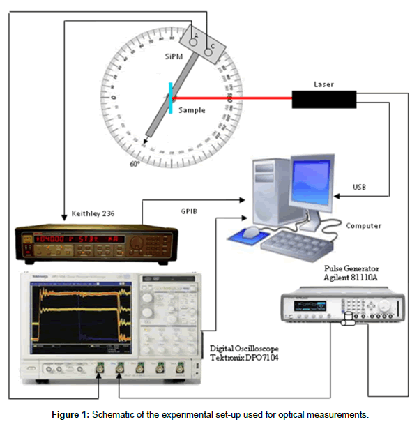
The set up for optical measurements [23], schematically reported in Figure 1, consisted of a light source provided by a Coherent Laser Cube at 660 nm impinging normally the sample, an optical filter (-30dB), a Keithley 236 source meter unit (SMU) to bias the SiPM and collect the signal through an electrical filter (when the measurement was performed in continuous mode), a goniometer, to change the detector/ sample angle (we used 60° mostly), a digital oscilloscope (Tektronix DPO7104, BW 1GHz) to detect the signal when the device operation was pulsed. A pulse generator (Agilent 81110A) was used to electrically modulate the excitation laser using a square waveform with period of 10 ms and width of 3.9 ns. All measurements were performed, and the data collected, using an automated data acquisition set-up developed for this purpose using a Labview© software. Two different positions for the detector were used: at 60° for Cy5 detection and at 180° (along the laser beam line) for Ru(bpy)32+ detection.
Electrical measurements were carried out at room temperature (RT) using drops of PBS buffer solutions to provide the upper contact of the MOS-like structure having the organic layer combined with SiO2 as dielectric. The electrical signal was generated by a Tektronics AWG2005 wave generator, measured using a BOONTON capacitance meter (1 MHz small signal), and collected by a TDS520B oscilloscope. Also in this case, the data were collected by a PC using a homemade program implemented with the Labview© software. Measurements were repeated to a frequency of 10 Hz in dark, to avoid photo induced carrier generation. The bias ranged from +2V to -2V. Each set of measurements (consisting in 120 CV curves) was performed at least three times. A C/ Cox value of 0.87 was used as reference point. The corresponding voltage value was used to determine the voltage shifts among the different samples.
Results and Discussion
Optical transduction method
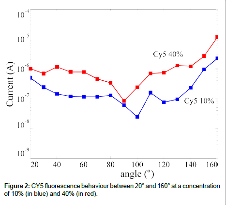
In optical transduction the DNA probe is spotted on a non-active surface since the detector can be physically separated from the sensing layer. The spotting methods on glass surfaces are well established, hence our research focused on the fluorescence signal provided by the DNA target (functionalized with fluorophores). Aim of our work was to define if the SiPMs used were able to detect the florescence signal of a common dye, we used the CY5, and if a different dye could be used as well. The experimental set-up we used, the components are described before, is schematically shown in Figure 1 [23]. We tested the emission signal as a function of both the detection angle and the fluorophore concentration in the sample. Some of the results are summarized in Figure 2, where the emitted signal is reported as a function of the detection angle. It should be mentioned that the 180° angle cannot provide useful information since the fluorophore emission and the laser signal are too close to be separated by a filter, hence the data are reported up to 160°. The data reported in figure are obtained subtracting the reference signal to the observed one; hence they are only due to the fluorophore emission. Both the dark signal (due to the device dark current) and the reflections (laser reflection on the sample that could reach the detector) are subtracted using this procedure. It is clearly visible a signal reduction in the range 90-100° for the two concentration showed (10% and 40%), as expected, being at the edge of the coverslip (Figure 1). The signal value is roughly constant in the full measurement range (with the exception just mentioned), confirming the isotropic emission nature of the fluorescence signal. Another feature observed in figure is the difference in the signal height at the two concentrations, being the signal higher at the highest concentration.
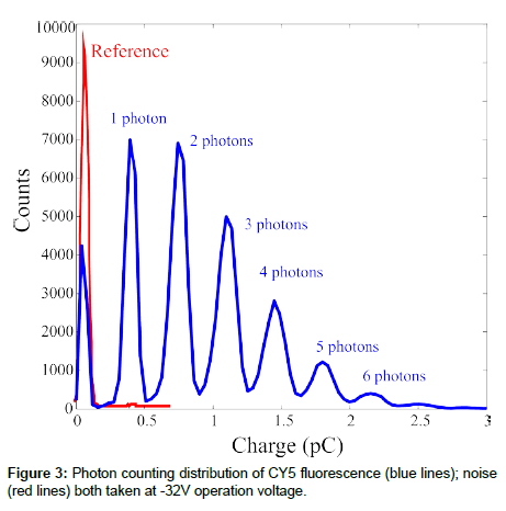
Once we have shown the SiPM ability to detect the fluorescence signal, we studied the possibility to use the device as a photon counter. For this reason we used an oscilloscope to collect both the reference signal (dark count and laser reflections, see before) and the fluorescence signal. The results are compared in Figure 3. The dots are the noise signal measured from the reference sample. It is clear the presence of only one peak due noise. Once the CY5 sample was shined, we observed seven peaks, the last barely visible in figure, at different amplitudes due to the arrival of up to 7 photons, on average, on 7 different pixels at the same time. The peaks separation in the photoelectron spectrum measured can be directly related to the charge delivered by one pixel once fired, ~ 3.50·10-13 C. Assuming nph=1, the SiPM gain was estimated to be about 2.2·106, at -32 V bias voltage (the operation voltage used for the measurements shown in Figure 3). The result is confirmed by literature data on the same samples [5]. The results just shown demonstrate that the SiPM can operate in photon counting and its sensitivity when a traditional fluorophore is used.
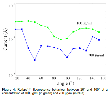
SiPM was also used to study innovative fuorophore optical behaviour. In particular, we used Ru(bpy)3, that exhibits an absorption peak at 450 nm and an emission peak at 630 nm [24]. Two interesting characteristics drove us in the choice of this fluorophore: the wide distance between the absorption and emission peaks, more than 100 nm; the “long”, compared to traditional fluorophores, emission lifetime, ~350 ns. Also using this fluorophore we made a detected current versus angle characterization of the emitted signal as a function of the concentration and the results are summarized in Figure 4. The fluorescence signal, obtained as mentioned before for the CY5 signal (Figure 2), has an isotropic emission, as expected, but, in this case, the sample at the lowest fluorophore concentration exhibits the highest emission signal. Further measurements are in progress to explain the obtained data.
The results so far shown indicate that the silicon photomultiplier can be usefully employed to detect the fluorescence signal using common fluorophores; hence it could efficiently replace the traditional scanner or imager to collect the optical signal. The use of such Si-based device, could allow a further integration of the detector in the reading system, thus allowing a further miniaturization of the whole system. Moreover, the possibility to use it as a photon counter, able to detect even single photons, could allow reducing the solution volumes and DNA concentration within the solutions. It is known that state-of-theart analysis requires a polymerase chain reaction (PCR) amplification of the DNA target. Out detection system could strongly reduce the number, thus reducing the sample preparation procedures. Finally, the use of a different fluorophore, having a large difference between the excitation and the emission wavelengths, could allow to strongly modifying the detection system, also allowing studying the possibility to use other detection parameters, such as the fluorophore lifetime.
Electrical transduction
The fabrication of a biosensor having an electrical transduction mechanism must face three main issues: the correct device functionalization, i.e. the “inorganic” device element must keep its electrical functionality; the correct biological molecule immobilization, since also the “organic” part of the biosensor must keep its functionality; and the transduction effectiveness.
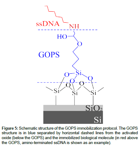
In order to address the first point, we optimized two main immobilization protocols, the differences being dependent from the silane used. The main characteristics of both can be found [17]. Hereafter, the main characteristic of the immobilization protocol we used in this work are summarized and a schematic of the full protocol is reported in Figure 5. It consists of the following steps: i) Surface cleaning by oxydation and hydroxyl activation; ii) silanization; iii) deposition and anchoring of oligonucleotides-DNA; iv) Blocking of the active surface. The first step is accomplished by dipping the sample into an oxidizing solution (H2O:H2O2:NH4OH) followed by an immersion in an acid solution (HCl:CH3OH) that has been demonstrated to be very effective to this purpose [17]. The oxidizing solution, that can be detrimental for the device metallization can be skipped if the oxide is “just grown”. In fact, this step is used only to clean the oxide surface, since the oxide activation is demanded to the acid solution. After that, before silanization, an anhydrification phase was carried out in order to remove any traces of surface water which negatively affects the silane coupling to Si-OH surface terminations. The second step consisted in the grafting of the 3-glycidoxypropryltrimethoxysilane (GOPS) onto the previously activated oxide surface. The organosilane epoxy ring (head group) is very reactive toward nucleophiles such as amines, thiols, alcohols, and acids, and was used to immobilize the biomolecules having a free amino group (ssDNA are terminated with an amino group). It should be mentioned that the grafting step must be carried out in anhydrous solvent (toluene) since the presence of water, even in traces, may cause silane polymerization, thus reducing the silane capabilities to anchor the biological molecules and would result in an inhomogeneous monolayer formation. After silanization, GOx was immobilized through a sample immersion overnight, while ssDNA oligos probes were firstly spotted and then covalently anchored to the glyxidoxy-derivatised surface. Finally, to saturate all the unreacted glycidoxy groups on the surface, a final blocking step using BSA (Bovine Serum Albumin) may be carried out. The main reason of the protocol choice resides in the first immobilization step. As mentioned earlier, the solution used to clean the oxide surface can be avoided if the oxide is “as prepared”. The possibility to skip this step allows one to preserve fully ULSI compatibility. In fact, the cleaning procedure on a metalized device would result in the removal (partial or full, depending on the solution concentration and dipping times) of the aluminum metal layer, regardless of its thickness. A schematic of the immobilization protocol used is shown in Figure 1 [17]. Unfortunately, the solution found does not allow one to fully solve issue of the inorganic device electrical functionality, as it will be shown in the “electrical transduction” section.
Many measurements were performed to verify if the immobilization protocols may affect the biological molecule functionality using GOx as reference [17,25,26], while for DNA, the functionality is preserved if it keeps its ability to hybridize the complementary strand.
In order to address the last point, i.e. the effectiveness of the transduction mechanisms, we used MOS-like, biosensor structures [27]. The sample structure (see experimental) is an EIS (Electrolyteinsulator– semiconductor) device. Capacitance vs voltage (CV) measurements provide, for this kind of structure, information about the insulator–solution interface. A chemical modification of this boundary, like the immobilization of a biological molecule or the hybridization of a complementary strand should result in a capacitance variation that will depend on the nature and coverage of the modification material. In fact, if the bio-recognition element does not completely cover the electrodes the results may be affected by the presence of “voids”, i.e. region without the sensing layer, where the solution come in direct contact with the inorganic surface.
The capacitance is given by the series of three main capacitors: the semiconductor/insulator capacitance (CS/I) that will depend only from the “inorganic” part of the device; the capacitance due to the biological sensing molecule (our probe, i.e. in DNA hybridization the ssDNA having the known basis sequence) to the Stern layer consisting of hydrophobically bound water molecules between the recognition and the diffuse layers and, eventually, to the recognized analyte [17] (Cprobe); the capacitance given by the region spanning from the outer device surface and the bulk of the solution (CInt) [28]. The total capacitance CTot, is then: 1/CTot=1/CS/I+1/Cprobe+1/CInt. Such equation clearly states that the lowest capacitance will dominate the total capacitance. The design rules are, then, the trade-off between the need to have a high insulating layer capacitance to lower its contribution (high oxide thickness), and the need to have a high sensitivity, hence a thin oxide. The recognition event will cause a shift in the normalized capacitance curve that can easily determine monitoring the voltage difference at a fixed C/Cox value.
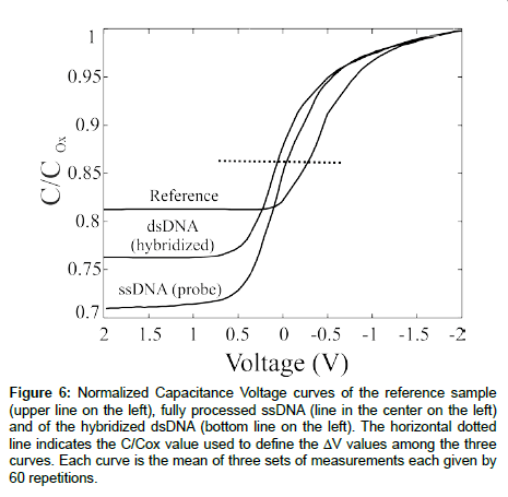
A full set of samples, consisting in a reference, a probe-anchored and a full match sample, was electrically tested (see experimental) and the results are summarized in Figure 6. The reference sample was a SiO2 15 nm thick, grown on Si. We graphically determined the VFB value (see the dotted line in Figure 6) as -0.41 ± 0.03 V. The results are the average of ~500 CV curves. The probe-anchored sample was obtained performing the immobilization protocol just described and anchoring single strand DNA as probe. The correct DNA immobilization was verified by different techniques [16,17]. A clear shift of the CV characteristics can be observed, suggesting that the DNA negative charge modifies the VFB value. In fact, within a solution, DNA molecules are known to have negative charges derived from their phosphate groups, hence a negative charge was trapped on the sample surface, producing a positive shift in the CV curves. The perfect match sample was obtained allowing to the probe-anchored sample to interact with the perfect match target. The hybridization process produced a further shift of the VFB value. The data show a VFB value of +0.06 ± 0.01 V after the device full processing, about 0.5 V shift with respect to the reference sample.
Figure 6: Normalized Capacitance Voltage curves of the reference sample (upper line on the left), fully processed ssDNA (line in the center on the left) and of the hybridized dsDNA (bottom line on the left). The horizontal dotted line indicates the C/Cox value used to define the ΔV values among the three curves. Each curve is the mean of three sets of measurements each given by 60 repetitions.
Further considerations can be obtained from the CV curves just described. According to the theory, the ratio Ctot/Cox in the inversion region should be _~ 0.2, much lower than the values experimentally observed, lying between 0.7 and 0.8. The strong deviation from the expected results is due to a high concentration of ions (H+, Na+) that can migrate from the solution to the semiconductor/dielectric interface. A full discussion can be found [16]. Moreover, the data inspection allowed us to observe that the DNA immobilization causes a visible reduction in the CMin value and the DNA layer thickness can be inferred from these measurement following the calculation assuming a dielectric constant for the biological layer of 3 [29]. A value of ~5.6 nm was obtained, in good agreement with the ssDNA length (6.8 nm). The most important conclusion that can be drawn from these data is that this device is very sensitive to the presence of organic layers, hence it is a promising candidate for the fabrication of fully electric (MOS-based) biosensors.
The possibility to use a “simple” MOS-like structure could be very helpful if either a low cost device or a strong device miniaturization is required. In fact, MOS-like sensors could be easily integrated in complex microelectronic circuits, without modifications of the fabrication rules. Finally, MOS-like structures could perform multiple electrical measurements during the same recognition event, thus obtaining more information and the noise minimization.
Conclusion
The main results obtained from our research team on Si-based biosensors were reported. We defined two different transduction mechanisms, optical and electrical, and focused our research on the fabrication and characterization of devices and systems that could be useful for biosensing applications. The use of silicon photomultipliers, produced by the Research & Development of STMicroelectronics of Catania, as optical detector for both traditional (Cy5) and innovative [Ru(bpy)3 2+] fluorophores, was investigated. We showed the SiPM can easily detect the fluorescence emitted by the dyes allowing, thanks to the small device dimensions, to study the emission isotropy without moving the sample. Pulsed measurements performed on Cy5 emission allowed us to conclude that SiPM can be used as photon counter also for biosensing applications.
Electrical transduction of the bio-recognition event can be performed only if a proper immobilization protocol of the probe is achieved. We optimized a method able, in principle, to anchor every amino-terminated molecule, but the results shown in this paper are referred only to ssDNA immobilization. The electrical measurements reported clearly show that the proposed system is sensitive to the DNA presence and to the perfect match hybridization, but further studies are needed to avoid interference effects of the saline solution used to carry out the measurements.
Acknowledgements
This work has been funded by MIUR by means of the national Program PON R&C 2007-2013, project “Hyppocrates – Sviluppo di Micro e Nano-Tecnologie e Sistemi Avanzati per la Salute dell’uomo” (PON02 00355).
Fundings
MIUR by means of the national Program PON R&C 2007-2013, project “Hyppocrates – Sviluppo di Micro e Nano-Tecnologie e Sistemi Avanzati per la Salute dell’uomo” (PON02 00355).
References
- Schena M (2003) Microarray Analysis. John Wiley & Sons, New Jersey, USA.
- Davidsson R, Genin F, Bengtsson M, Laurell T, Emnéus J (2004) Microfluidic biosensing systems. Part I. Development and optimisation of enzymatic chemiluminescent micro-biosensors based on silicon microchips. Lab Chip 4: 481-487.
- Wang J (2000) From DNA biosensors to gene chips. Nucleic Acids Res 28: 3011-3016.
- Pagano R, Valvo G, Sanfilippo D, Libertino S, Corso D, et al. (2013) Silicon Photomultiplier Device Architecture with Dark Current Improved to the Ultimate Physical Limit. Appl Phys Lett 102: 183502.
- Pagano R, Libertino S, Corso D, Lombardo S, Valvo G, et al. (2013) Silicon Photomultiplier: Technology improvement and performance. International Journal of advances in System Measurements 6: 124-136.
- Santangelo MF, Pagano R, Lombardo S, Sciuto EL, Sanfilippo DN, et al. (2014) Silicon photomultipliers applications to biosensors. Silicon optoelectronic devices IX, Proc. SPIE 899027, San Francisco, California, United States.
- Berggren C, Bjarnason B, Johansson G (2001) Capacitive biosensors. Electroanalysis 13: 173-180.
- Sakata T, Kamahori M, Miyahara Y (2004) Immobilization of oligonucleotide probes on Si3N4 surface and its application to genetic field effect transistor. Mat Sci Engineer C 24: 827-832.
- Schöning MJ, Poghossian A (2006) Bio FEDs (Field-Effect Devices): State-of-the-Art and New Directions. Electroanalysis 18: 1893-1900.
- Spinke J, Liley M, Schmitt FJ, Guder HJ, Angermaier L, et al. (1993) Molecular recognition at self-assembled monolayers: Optimization of surface functionalization. J Chem Phys 99: 7012-7019.
- Voicu R, Boukherroub R, Bartzoka V, Ward T, Wojtyk JT, et al. (2004) Formation, characterization, and chemistry of undecanoic acid-terminated silicon surfaces: patterning and immobilization of DNA. Langmuir 20: 11713-11720.
- Zammatteo N, Jeanmart L, Hamels S, Courtois S, Louette P, et al. (2000) Comparison between different strategies of covalent attachment of DNA to glass surfaces to build DNA microarrays. Anal Biochem 280: 143-150.
- Boukherroub R, Wayner DDM (1999) Controlled Functionalization and Multistep Chemical Manipulation of Covalently Modified Si(111) Surfaces. J Am Chem Soc 121: 11513-11515.
- Falconnet D, Csucs G, Grandin HM, Textor M (2006) Surface engineering approaches to micropattern surfaces for cell-based assays. Biomaterials 27: 3044-3063.
- Knoll W (1998) Interfaces and thin films as seen by bound electromagnetic waves. Annu Rev Phys Chem 49: 569-638.
- Libertino S, Cannella G, Aiello V, Busacca A, Lombardo S (2012) Electrical characterization of DNA hybridization in MOS-like structures. Appl Phys Lett 101: 093703.
- Libertino S, Conoci S, Scandurra A, Spinella RC (2013) Biosensor integration on Si-based devices: feasibility studies and example. Sensors & Actuators B: Chemical 179: 240-251.
- Libertino S, Giannazzo F, Aiello V, Scandurra A, Sinatra F, et al. (2008) XPS and AFM characterization of the enzyme glucose oxidase immobilized on SiO(2) surfaces. Langmuir 24: 1965-1972.
- Hecht HJ, Kalisz HM, Hendle J, Schmid RD, Schomburg D (1993) Crystal structure of glucose oxidase from Aspergillus niger refined at 2.3 A resolution. J Mol Biol 229: 153-172.
- Wilson R (1992) Glucose oxidase: an ideal enzyme. Biosens Bioelectron 7: 165-185.
- Mazzillo M, Condorelli G, Sanfilippo D, Valvo G, Carbone B, et al. (2009) Silicon Photomultiplier Technology at STMicroelectronics. IEEE Trans Nucl Sci 56: 2434-2442.
- Libertino S, Corso D, Lisiansky M, Roizin Y, Palumbo F, et al. (2012) Ionizing radiation effects on Non Volatile Read Only Memory cells. IEEE transaction on Nuclear Science 59: 3016-3020.
- Santangelo MF, Pagano R, Sciuto EL, Lombardo S, Sanfilippo DN, et al. (2013) CY5 fluorescence measured with Silicon photomultipliers. Biosensors & Bioelectronics.
- Kalyanasundaram K (1982) Photophysics, photochemistry and solar energy conversion with tris(bipyridyl)ruthenium(II) and its analogues. Coord Chem Rev 46: 159-244.
- Libertino S, Fichera M, Aiello V, Statello G, Fiorenza P, et al. (2007) Experimental characterization of proteins immobilized on Si-based materials. Microelect Eng 84: 468-473.
- Libertino S, Scandurra A, Aiello V, Giannazzo F, Sinatra F, et al. (2007) Layer uniformity in glucose oxidase immobilization on SiO2 surfaces. Appl Surf Sci 253: 9116-9123.
- Libertino S, Fichera M, Aiello V, Lombardo S, Scandurra A, et al. (2008) Electrical characterization of biological molecules deposition in MOS capacitors. Sensor Letters 6: 531-536.
- Hadzifejzovic E, Stankovic J, Firth S, McMillan PF, Caruana DJ (2007) Plasma electrochemistry: electroreduction in a flame. Phys Chem Chem Phys 9: 5335-5339.
- Bataillard P, Gardies F, Jaffrezic-Renault N, Martelet C, Colin B, et al. (1988) Direct detection of immunospecies by capacitance measurements. Anal Chem 60: 2374-2379.
Relevant Topics
Recommended Journals
Article Tools
Article Usage
- Total views: 14252
- [From(publication date):
specialissue-2014 - Apr 04, 2025] - Breakdown by view type
- HTML page views : 9665
- PDF downloads : 4587

