Research Article Open Access
On-Chip Interconnect mechanism based on CDMA
Vijaya Kumar P*, Rajesh VDepartment of ECE, Faculty of Engineering & Technology. SRM University, Chennai
- *Corresponding Author:
- Vijaya Kumar P
Department of ECE, Faculty of Engineering & Technology. SRM University, Chennai
E-mail: vijay_at23@rediffmail.com
Visit for more related articles at International Journal of Advance Innovations, Thoughts & Ideas
Abstract
The integration of complete Network-on-chip (NoC) designs consisting of large number of Intellectual Property (IP) blocks (cores) on the same silicon die is becoming technically feasible. But, the communication between the IP Cores is the main issue in recent years. This paper presents an On-Chip interconnect mechanism as a component of Code Division Multiple Access (CDMA) for shared bus architecture to communicate between IP cores in SoC. In the proposal, only bus lines that carry address and data signals are CDMA coded. CDMA technology has better channel isolation, channel continuity, data integrity and also reduces the number of lines in the shared bus for transmitting the data from master to slave
Keywords
CDMA, On-Chip interconnects, Shared Bus Architecture.
Introduction
The SoC (System on Chip) consists of a heterogeneous mix of components and functional units that tailors towards the specific application domains. The increasing number of IP cores that can be integrated on a single chip enables implementation of complex applications using SoC. As more and more components are integrated into an on-chip system, communication issues become complicated. [1] Network-on-chip (NoC) is proposed to solve the On-Chip communication problems.
Traditional system level design aims at designing reliable single function systems or distributed embedded systems. However, the design complexity exponentially grows as the number of functions on one chip increases. Traditional approach is not suitable for such systems. As the number of components on single chip and their performance continue to increase, a shift from computation based to communication based design is becomes mandatory. As a result, the communication architecture plays a major role in the area, performance and energy consumption of overall system.
There are two types of on-chip communication schemes have been considered, namely point-top point (P2P) and bus based communication architectures, P2P communication architectures can provide the utmost in communication performance at the expense of dedicated channels among all the communicating IP pairs. However these architectures suffer from lack of scalability in terms of high complexity, cost and design effort. On the other hand, bus based architectures can connect a few tens of IP cores in a cost-efficient manner by reducing the design complexity and eliminates the dedicated wires required by P2P communication architectures. However, bus-based architectures still fail to satisfy the requirements of future applications mainly due to lack of scalability both in terms of energy and performance.
In contrast to these methods, the Network-on-Chip approach emerged as a promising solution to on chip communication problems. In order to eliminate variance of data transfer latency and complexity incurred by routing issues in a P2P connected NoC, [1] an On-Chip network which applies a code division multiple access (CDMA) technique is introduced in this paper. As one of the spread-spectrum techniques, CDMA technique has been widely used in wireless communication systems because it has great bandwidth efficiency and multiple access capability .CDMA technique applies a set of orthogonal codes to encode the data from different users before transmission in shared communication media. Therefore it permits multiple users to use the communication media concurrently by separating data from different users. [2] CDMA NoC is helpful for providing a guaranteed communication service for on-chip system. Rest of the paper is organized as follows. In section II explains about the CDMA Interconnect mechanism. Section III describes the design solution and related work. Section IV about experimental results and in Section V discusses conclusions.
CDMA Technology
CDMA technology is based on the principle of orthogonally, when a multiple code words are summed; they do not interfere completely with each other at every point of time and can be separated without loss of information. Digital code words are consists of a series of bits which is generated by linear feedback shift register (LFSR) so that sequences repeats only at every (2N -1) clocks, Where N is the number of bits in the shift register. Sender modulates the data bit with the specific (2N -1) code bits unique to particular receiver. The modulated bits from different sources can be summed together using parallel counter. These results will ranges from - (2N -1) to (2N -1) and are transmitted. CDMA has been widely used for wireless communications. The summed mixture goes through an up-conversion process which translates the frequency to higher band. But for digital bus interconnects, there is no need for up-conversion or down-conversion. However the nature of summation prevents the results from being purely binary.
A. The CDMA digital bus
In CDMA digital bus bits are represented as +1 or -1 after modulation with the LFSR sequence and summation. This implies that log2 N pure information bits require log2 (N+1) transmission bits.
B. The Binary CDMA bus
The Binary CDMA Bus avoids the multiple-valued representations by encoding the summations. The summations that are less than 0 are ignored. [3] The summer counts the number chips that are greater than 0 and transmits the binary equivalent. For 255 processors only summations from 0 to 255 or 8 equivalent information bits are needed. At the receiver side the original summation from -255 to 255 is reconstructed for the transmitted value P (summed value), the orthogonal summation is (2P-255).CDMA Encoding scheme is shown in the Fig.1.

Figure 1: CDMA Encoding Scheme
C. CDMA Code words
Since the code length is the bandwidth multiplying factor and the number of available codes is the bandwidth dividing factor, it is desirable to have the code word in large number for small number of chips. CDMA transmitter is described in the following Fig.2

Figure 2: CDMA encoding using Code words of length 8
Related Work
In order to send the n-bits of data through the shared bus architecture we require n-bits of lines. But, the CDMA technology reduces the number of lines required lines for sending n-bits through the shared bus. Let us consider the length of the code word is S and then un-encoded buses are of n-bits width then the CDMA coded equivalent buses will be reduced to P=n/s [log2 S + 1]. For 8-bit spreading code a bus reduction is 50%. Table 1 shows the average bus reduction using the CDMA.

Table 1: NO.OF LINES REDUCED FOR “S‟ AND “n‟ BY CDMA
CDMA Encoding is done for 32-bit data using 8-bit length of different spreading code words. Code words are generated by using 8-bit LFSR. To give great orthogonality, taps for the LFSR is taken at 1,2,3,7 registers in an 8-bit shift register and the XOR of these taps are given as the input for the first register. Output of LFSR is taken parallelly at each register, which will look like SIPO shift register.
Experimental Results
Increasing demand for high-speed on-chip interconnects requires faster links that consumes less power. An on-chip interconnect based on CDMA technique of relatively low complexity, low power and high bandwidth is proposed here and its performance related to design of CDMA are evaluated.
The CDMA Technique was described in RTL Level using VHDL. For Synthesis QUARTUS 11.0v [7] was used and for simulation MODELSIM 10.0c was used. The simulation results for the CDMA Encoding is shown in the Fig.3

Figure 3: Simulation results of CDMA Encoding Scheme
Conclusion
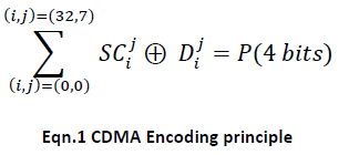
In this paper we have shown that CDMA encoding technology for the data from the NIOS II processor has been described by using the below principle as shown in Eqn.1 for NoC architecture to decrease the number of lines required to transfers the data. This encoding scheme is only applicable to address and the data buses and not for the control lines. So that we can greatly achieve the data integrity, and greater bandwidth of shared bus architecture. Where “SC” is spreading code, “D” is the data bit, and “P” the output.
References
- Vincenzo Rana, David Atienza, Macro Domenico Santambrogio, Donatella Sciuto and Giovanni De Micheli, “A Reconfigurable Network-on-Chip Architecture for Optimal Multi-Processor SoC Communication” IFIP, VLSI-SoC 2010, pp.232-250.
- Yasushi Yuminaka, Osamu Katoh, Yoshisato Sasaki, Takaf-umi Aoki, Tatsuo Higuchi, “An Efficient Data Transmission
- X. Wang, T. Ahonen, and J. Nurmi, “Applying CDMA Technique to Network-on-Chip”, IEEE Transactions On Very Large
- Cheng-Min Lien, Ya-Shu Chen, and Chi-Sheng Shih, “On-Chip Bus Architecture for Multi-core SoC Systems”, IFIP
- Abhijit Athavale and Carl Christen, “High Speed Serial Made Simple”, 1st Ed, Xilinx Inc, Apr 2005.
- Men-Chow Chiang, Gurinder S. Sohi, “Evaluating Design Choices for Shared Bus Multiprocessor in a Throughputoriented
- Quartus II Device Support, Altera Inc, May 2008.
- Avalon Bus Specification, Reference Manual, Altera Inc, July 2002.
- Francesco Poletti, Davide Bertozzi, Luca Benini, and Alessandro Bogliolo,”Performance Analysis pf arbitration polices for
- Terrence S. T. Mak, N. Pete Sedcole, Peter Y. K. Cheung, Wayne Luk , “On FPGA Communication Architectures and
- On-chip Bus Development Working Group, “Virtual Component Interface Standard Version 2”, April 2001.
- A. Athavale, C. Christensen, High-Speed Serial I/O Made Simple, Xilinx Connectivity Solutions, San Jose, April 2005
Relevant Topics
- Advance Techniques in cancer treatments
- Advanced Techniques in Rehabilitation
- Artificial Intelligence
- Blockchain Technology
- Diabetes care
- Digital Transformation
- Innovations & Tends in Pharma
- Innovations in Diagnosis & Treatment
- Innovations in Immunology
- Innovations in Neuroscience
- Innovations in ophthalmology
- Life Science and Brain research
- Machine Learning
- New inventions & Patents
- Quantum Computing
Recommended Journals
Article Tools
Article Usage
- Total views: 13896
- [From(publication date):
May-2012 - Apr 11, 2025] - Breakdown by view type
- HTML page views : 9304
- PDF downloads : 4592