Review Article Open Access
Nanomaterial-modified Flexible Micro-electrode Array by Electrophoretic Deposition of Carbon Nanotubes
Winkin N1*, Gierth U2, Mokwa W1 and Schneider M21RWTH Aachen University, Institute of Materials in Electrical Engineering, Sommerfeldstraße, Achen, Germany
2Fraunhofer Institute for Ceramic Technologies and Systems IKTS, Electrochemistry, interbergstraße 28, Dresden, Germany
- Corresponding Author:
- Winkin N
RWTH Aachen University
Institute of Materials in Electrical Engineering
Sommerfeldstraße 24, 52074 Aachen, Germany
E-mail: winkin@iwe1.rwth-aachen.de
Received date: April 21, 2016; Accepted date: May 25, 2016; Published date: June 02, 2016
Citation: Winkin N, Gierth U, Mokwa W, Schneider M (2016) Nanomaterial-modified Flexible Micro-electrode Array by Electrophoretic Deposition of Carbon Nanotubes. Biochip Tissue Chip 6:115. doi:10.4172/2153-0777.1000115
Copyright: © 2016 Winkin N, et al. This is an open-access article distributed under the terms of the Creative Commons Attribution License, which permits unrestricted use, distribution, and reproduction in any medium, provided the original author and source are credited.
Visit for more related articles at Journal of Bioengineering and Bioelectronics
Abstract
Micro-electrode arrays (MEAs) and micro-electrodes are used in a variety of medical applications for recording action potentials or stimulating neurons. To have an excellent signal-to-noise ratio, the contact between the neuronal tissue and the micro-electrodes must be very close. Therefore, a flexible MEA with a large number of electrodes on a large area is necessary. In this work, a flexible micro-electrode array (MEA) with an integrated flexible CMOS-chip was designed and fabricated. By connecting several of these MEAs by a bus system, the number of electrodes and therefore the spatial resolution can be increased extremely. Because of the small size of the micro-electrodes (<120 µm) each electrode needs a high charge delivery capacity and a high “true” surface area for stimulation, respectively. This can be obtained by coating the electrodes by disordered multi-walled carbon nanotubes (MWCNTs). Direct current pulsed Electrophoretic Deposition (EPD) has been proved successfully for the aforementioned application. The effective deposition time and the pulse width were figured out to create ideal MWCNT-electrode properties, particularly, with regard to the enhancement of the “true” surface area, microscopic homogeneity and reproducibility of the layer.
Keywords
Micro-electrodes; Flexible micro-electrode array; Multiwalled carbon nanotubes; Electrophoretic deposition
Introduction
Micro-electrodes and micro-electrode arrays (MEAs) are very important in a variety of medical applications like cochlear implants, retinal implants or deep brain stimulators. There, micro-electrodes are used for recording action potentials or stimulating neurons [1]. Especially for retinal implants it is necessary that these MEAs are flexible to conform to the curvature of the eye. So far, the diameter of an electrode array in retinal implants is in the range of 6 mm [2-4] and therefore the field of vision is very limited. Wide-field retinal implants must have a diameter of more than 10 mm which corresponds to a vision of field greater than 34° [5]. Moreover, the number of electrodes is a very important point to increase the local resolution significantly. Currently, the Argus II epiretinal prosthesis system shows the highest electrode number. It has 60 platinum electrodes on a flexible polyimide substrate which are connected to the control electronics via metal lines. The electrodes are arranged in a 6 × 10 grid and cover about 20° of the visual field (diagonally) [6]. Chader et al. estimate that a MEA with approximately 1000 electrodes could give good functional vision as reading ability and face recognition [7]. But such high numbers of electrodes can no longer be connected via single metal lines to the electronic components. For that reason, the electronics must be very close to the electrodes. This approach is followed by the Retina Implant AG in Germany. Their subretinal implant consists of an array of 1500 active photodiodes, each with his amplifier and local stimulation electrode [3]. Electrodes and electronics are on a single CMOS-chip, having a size of 3 mm × 3.1 mm. But this implant is non-flexible and has a very small sight of view. A purely optical subretinal prosthesis was developed by Palanker et al. [8]. This prosthetic system has an array of silicon islands which are connected via flexible silicon membranes. Photodiodes on the top of the islands could be activated from infrared light from the outside. In this way stimulation currents were generated. Viventi et al. developed flexible foldable high-density arrays for mapping brain activity in vivo [9]. Very thin silicon membranes (260 nm) were used for realization of 720 transistors to map neural activity on the surface of visual cortex. The circuitry and the transistors are fabricated in a complex non-standard process. Therefore, it is not possible to use state-of-the-art CMOS.
To increase the density of electrodes significantly, means to decrease the diameter of the electrodes, too. Electrode miniaturization is only reasonable when the electrical and electrochemical properties can be improved at the same time. Therefore, the electrodes have to be nanomaterial-modified. To have a high number of nano-modified electrodes, for example 1000 electrodes, means currently to have the same number of 1000 conductor lines to control them each individually. That is technically too extensive.
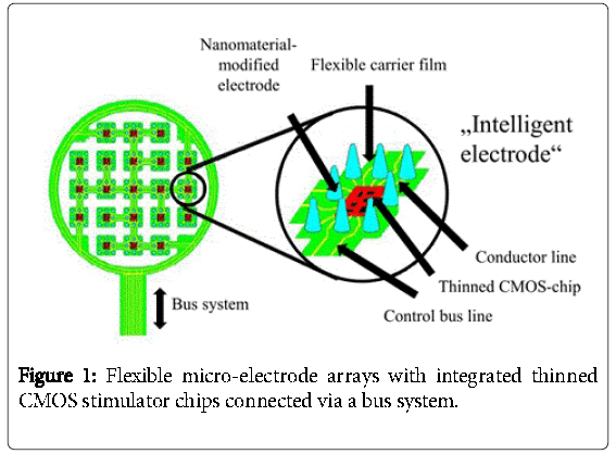
The idea of our work is to control these nanomaterial-modified electrodes with intelligent state-of-the-art CMOS circuits, which means that each circuit for example connects locally to 25 electrodes as shown in Figure 1. Then, several of these CMOS circuits could be connected and addressed via a bus system.
For this to work, the whole system has to be embedded into a flexible polyimide foil for better adaption to the human body. For this reason, the integrated chips must be flexible, too. This can be achieved by thinning the chip to a thickness below 40 μm. In this publication the design and fabrication steps of such an “intelligent electrode” will be presented. Furthermore, alternative coating of platinum electrodes with carbon nanotubes by electrophoresis has been investigated and will be presented. It is reported that carbon nanotubes are biocompatible [10].
Experimental
Design of Flex-MEA
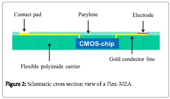
A schematic cross section of the system is shown in Figure 2. An ultrathin flexible CMOS-chip is embedded and encapsulated in a flexible polyimide carrier. The CMOS –chip used in our work is the same one which was used in the epiretinal implant of Rössler, et al. [4]. With this chip, programmable stimulation pulses for 25 electrodes can be controlled. For electrical isolation, the flexible micro-electrode array, called Flex-MEA, gets a final coating with parylene C.
Fabrication of flex-MEA
Flex-MEA was fabricated on an oxidized 4” silicon wafer. This wafer only served as a substrate to use standard wafer level processes. It was first coated with 50 nm titanium, 1 μm aluminum and 150 nm titanium. The first titanium on top of the silicon wafer served as an adhesion layer for the aluminum. The aluminum itself served as a sacrificial layer to separate in a final step the finished Flex-MEA from the wafer. The second titanium layer protected the aluminum layer from unwanted etching attacks during subsequent processing steps.
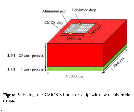
First, 1 μm of photo sensitive liquid polyimide “PI 2611” (HD MicroSystems Inc.) was spin-coated onto the metal layers. The polyimide has excellent biostability and biocompatibility as shown in [11]. After photolithography and wet chemical patterning, polyimide carriers with a size of 7000 μm × 7000 μm × 1 μm were defined to form the base structure of a Flex-MEA. These polyimide carriers (1.PI) had to be cured entirely in an oven at temperatures to 400°C under nitrogen atmosphere. Afterwards, the PI2611 was resistant to most solvents, bases and acids.
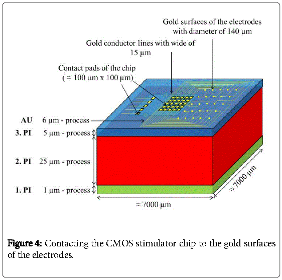
Then, a second polyimide layer (2.PI) with a thickness of 25 μm was deposited and a trench of about 2990 μm × 2600 μm × 25 μm was etched into the 2.PI. In a next step the CMOS stimulator chip, which was thinned on a lapping machine to 100 μm and after that dry-etched with sulfur hexafluoride to less than 40 μm, was placed into the trench. The CMOS-chip was centered and fixed in the trench with just two polyimide drops “on top” (Figure 3). The thickness of the two drops didn´t increase the total thickness because a third layer of 5 μm polyimide was spin coated on top to planarize the surface and to fully embed the CMOS stimulator chip into the polyimide. Then contact holes to the aluminum pads were processed by dry etching with oxygen. This third layer can be seen in Figure 4.
In a next step, 30 nm chromium and 100 nm gold were coated onto the whole wafer to serve as a plating base. Then, a resist mask that defined the pads, electrode-areas and gold conductor lines was applied and in a next step 6 μm of gold was electroplated. After that, the resist mask was removed with acetone and the plating base was etched away wet chemically. The pads, electrode-areas and conductor lines finally remained as shown in Figure 4.
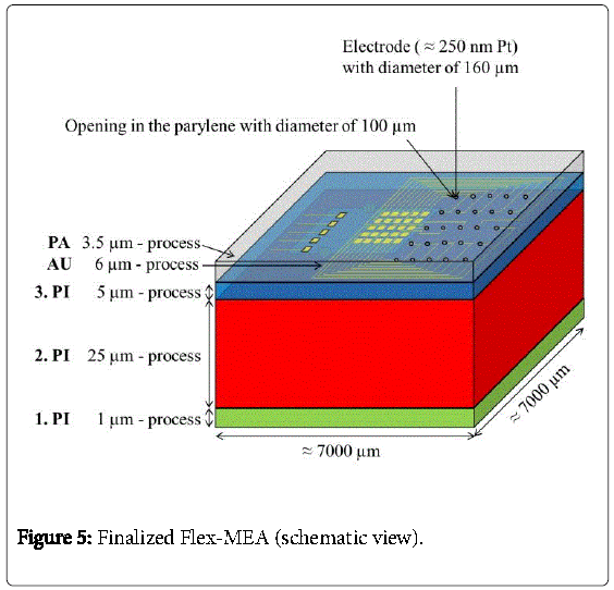
The gold-electrodes were then coated with 250 nm sputtered platinum (Pt). The platinum electrodes serve as stimulation electrodes. Finally, parylene C (PA) was deposited with a thickness of 3.5 μm for electrical isolation. Well-defined electrode openings of 100 μm in diameter were obtained by reactive dry etching of the parylene afterwards. The finalized Flex-MEA is shown in Figure 5.
Modification by Multi-walled carbon nanotubes (MWCNTs)
With increasing number of electrodes distributed over the whole MEA, the geometrical surface area of each single electrode has to decrease. In order to remain the electrical and chemical behavior, the required contact area between the electrode and the neuronal tissue has to be enlarged, so an increase of the “true” area is necessary [12]. The more of the contact area is formed, the higher is the electrode sensitivity e.g. charges delivery capacity.
Carbon nanotube (CNT) particles are extremely suited to bio sensing applications, due to the three dimensional structure, high aspect ratio, conductivity and biocompatibility [13-17]. Gaio et al. reported from the improvement of signal-to-noise ratio of recorded cell potential in case of CNT coated electrodes [1]. Furthermore, the wide inert electrochemical window represents a high advantage according to the measurement conditions.
Since the aforementioned parylene layer of Flex-MEA is only stable to temperatures of 125°C [18], the coating technic must carried out at significant lower temperatures. Therefore, electrophoretic deposition (EPD) is the prioritized method. EPD is a simple method for realizing fabrication of MWCNT electrodes, which allows implementation of CNT deposition at low temperatures as well as operating with aqueous solutions [19-21]. A pulsed direct voltage regime is also of major importance, due to bubble incorporation during EPD [22-24]. An effective deposition time and the pulse width were figured out in order to optimize electrode properties, particularly, with regard to the enhancement of the “true” surface area, microscopic homogeneity and reproducibility of EPD layer.
Measurements
The deposition of disordered MWCNTs (Baytubes C150 HP) was carried out by EPD in aqueous solution. According to product information the length of tubes after dispersion amounts to 0.1 – 0.2 μm. The inner diameter is specified between 2 - 6 nm and the outer diameter between 5 – 20 nm. The dispersion in aqueous solution requires a functionalization of the MWCNTs, which was realized by a pre-treatment of the MWCNTs in a stirred solution consisting of 65% HNO3 and 98% H2SO4 first at 60°C for 16 h and then at 110°C for 6 h. The original nonpolar MWCNTs were modified to polar particles, after functionalization it was enabled them to disperse and migrate in polar solvents. After filtration and washing, the suspension was dried at 70°C in air, cooled down and stored in a desiccator. The functionalized MWCNTs were dispersed in aqueous solution (c = 0.4 g/l) by ultrasonic disintegration. In earlier investigations, the particle size distribution of MWCNT in a water suspension was determined by the method of light scattering. The particle size ranges between 17 - 210 nm.
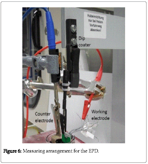
The Flex-MEA (working electrode) and a platinum grid (counter electrode) were dipped into the prepared dispersion (Figure 6). The electrode distance to the MEA amounted to 0.25 cm. A voltage of 4.2 V (field strength = 16.8 Vcm-1) was applied by a switching on/off-pulse regime. The EPD was realized by a power supplier (Elgar SW3700A). The extraction of the electrode from the dispension was carried out under a certain velocity using a dip coater (LTB 300, Walter Lemmen GmbH). Overall, 14 arrays with five electrodes each were deposited with MWCNTs. The pulse-on time (ton) and pulse-off time (toff) was varied, furthermore the effective time was investigated. The different parameters of the EPD are shown in Table 1.
| EPD parameter | teff(s) |
|---|---|
| toff = 5s; ton = 1s | 3; 4 |
| toff = 0.5s; ton =0.1s |
Table 1: Applied EPD parameter.
The sensitivity depends on the active or “true” surface area, which can significantly differ from the “geometric” area. Commonly, the “true” surface area can be calculated from the double layer capacitance (Cdl). The double layer capacitance was measured by electrochemical impedance spectroscopy (EIS), at the bare platinum electrode and after EPD (PGU IMP Micro, IPS – Peter Schrems) at the MWCNTelectrode. According to Equation 1, the capacitance (C) is directly proportional to the “true” surface area (A). Remaining parameters, such as plate distance (d) and dielectric permittivity (), were assumed to be constant. However, the authors only compare the differences in the measured double layer capacitance and estimated the enlargement of the active surface area expressed by a so-called roughness factor (Rf).
This roughness factor represents the surface magnification by MWCNTs in comparison to the smooth platinum surface. As shown in Equation 2, Rf is defined as a quotient of “true” and “geometric” surface area.
The EIS was carried out in 0.1 M potassium chloride, at 0 V versus open circuit potential. The amplitude was 20 mVpp. A saturated calomel electrode served as a reference, whereas a platinum grid worked as counter electrode.
Results and Discussion
The roughness factor establishes a comparison of the true surface area between a smooth platinum electrode and a rough MWCNTelectrode.
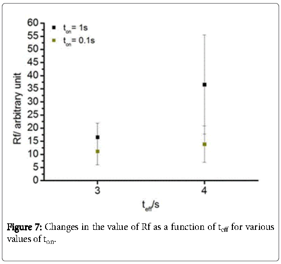
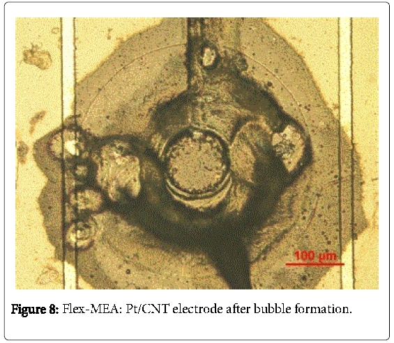
As indicated in Figure 7 the application of the pulse regime ton = 0.1 s shows similar values for Rf at teff = 3 s (11.2) as well as 4 s (13.9). However, the standard deviation (RF) is RF-3s = 5.1 and RF- 4s = 6.9. Likewise, using ton = 1 s shares the same values for teff = 3 s ( Rf = 16.6; RF = 5.3). In contrast, Rf (36.6) and RF (18.8) are significantly increased at teff = 4s. In general, the higher the effective time, the higher are the “true” surface areas. However, it leads also partially to an extremely high deviation. Furthermore, a microscopic inhomogeneity within the MWCNT layer is occurred predominantly at teff = 4 s regime (Figure 8). This phenomenon is caused by anodic oxygen evolution. The formation of bubbles is well known for deposition at high voltages in aqueous solution due to electrolysis of water. According to the literature, the current density increases with increasing deposition time. The longer the effective time, the more oxygen is generated.
Furthermore, the extent of electrolysis depends on the applied electric field [19,21,24]. Neirinck et al. describes that gas bubble formation can be avoided by using AC-EPD at high voltages and sufficiently high frequencies.
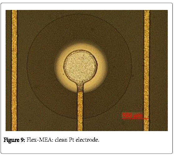
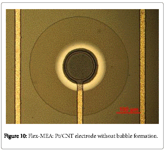
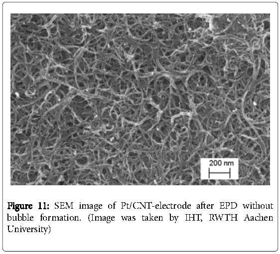
This is explained by an incomplete reloading of the electrochemical double layer and the suppression of the decomposition of water [25]. The reproducibility might be improved by using AC-EPD in further work. Buschhorn et al. have reported that the influence of different aspect ratios of MWCNT plays an important role on sensor properties (e.g. sensor conductivity) [17]. Nevertheless, generating a smooth homogeneous CNT surface was enabled at teff = 3 s and ton = 0.1 s as it is illustrated by a comparison between the cleaned and the CNTelectrode in Figures 9 and 10. Using the scanning electron microscopy (Figure 11), which was carried out over the whole electrode surface, the homogeneity is assumed. The results are in good agreement to the literature [26].
Conclusions
A novel flexible micro electrode array with an integrated CMOSchip was designed and successfully manufactured. Summarizing, it is possible to realize EPD of MWCNTs in an aqueous solution at microelectrode arrays of Pt. Microscopic homogenous smooth surfaces were generated. The best quality of microscopic homogeneity and reproducibility is affected by a pulse-on time of 0.1 s and an effective time of 3 s. The roughness factor amounts to 11.2 by a deviation of 5.1. This is due to the bubble formation during the EPD.
Acknowledgment
This work was supported by the German Federal Ministry of Education and Research (BMBF) under grant No. 16SV5322K.
References
- Gaio N, Meer BV, Silvestri C, Pakazad S, Vollebregt S, et al. (2015) Upside-down Carbon nanotube (CNT) micro-electrode array (MEA). Sensorspp:1-4.
- Kandagor V, Cela CJ, Sanders CA, Greenbaum E, Lazzi G, et al. (2010) In Situ Characterization of Stimulating Microelectrode Arrays: Study of an Idealized Structure Based on Argus II Retinal implants. in Biological and Medical Physics, Biomedical Engineering, Implantable Neural Prostheses2 139-156.
- Zrenner E, Ulrich KBS, Benav H, Besch D, Bruckmann A, et al. (2011) Subretinal electronic chips allow blind patients to read letters and combine them to words. Proceedings of The Royal Society 1711: 1489-1497.
- Roessler G, et al.(2009) Implantation and explantation of a wireless epiretinal retina implant device: observations during the EPIRET3 prospective clinical trial. Investigative ophthalmology & visual science 50: 3003-3008.
- Ameri H, Ratanapakorn T, Ufer S, Eckhardt H, Humayun MS, et al. (2009) Toward a wide-field retinal prosthesis. Journal of neural engineering 6: 35002.
- Zhou DD, Dorn JD, Greenberg RJ (2013) The Argus® II retinal prosthesis system: An overview, International Conference on Multimedia and Expo Workshops (ICMEW) pp:1-6.
- Chader GJ, Weiland J, Humayun MS (2009) Artificial vision: needs, functioning, and testing of a retinal electronic prosthesis. in Progress in Brain Research, Neurotherapy: Progress in Restorative Neuroscience and Neurology: Elsevierpp: 317-332.
- Palanker D, Vankov A, Huie P, Baccus S (2005) Design of a high-resolution optoelectronic retinal prosthesis. Journal of neural engineering 2: 1-20.
- Viventi J, Kim DH, Vigeland L, Frechette ES, Blanco JA, et al. (2011) Flexible, foldable, actively multiplexed, high-density electrode array for mapping brain activity in vivo. Nature neuroscience 14: 1599-1605.
- Etzkorn C, Johnen S, Meißner F, Endler I, P. Walter, et al. (2013) Different aligned multiwalled carbon nanotubes and their effects on cell viability and growth characteristics. Investigative ophthalmology & visual science.
- Stieglitz T, Beutel H, Schuettler M, Meyer JU (2000) Micromachined, Polyimide-based Devices for Flexible Neural Interfaces. Biomedical Microdevices 2: 283-294.
- Pizzi R, Cino G, Gelain F, Rossetti D, Vescovi A (2007) Learning in human neural networks on microelectrode arrays.Bio Systems 88: 1-15.
- Xiea XL, Maia YW, Zhou XP (2005) Dispersion and alignment of carbon nanotubes in polymer matrix: A review.Materials Science and Engineering: R: Reports49: 89-112.
- Minnikanti S, Skeath P, Peixoto N (2009) Electrochemical characterization of multi-walled carbon nanotube coated electrodes for biological applications.Carbon 47: 884-893.
- Li X, Liu X, Huang J, Fan Y, Cui FZ, (2011) Biomedical investigation of CNT based coatings.Surface and Coatings Technology 206: 759-766
- Lawal AT (2016) Synthesis and utilization of carbon nanotubes for fabrication of electrochemical biosensors.Materials Research Bulletin 73: 308-350.
- Buschhorn ST, Wichmann MH, Sumfleth J, Schulte K, PegelS, et al. (2011)Charakterisierung der Dispersionsgüte von Carbon Nanotubes in Polymer-Nanokompositen.ChemieIngenieurTechnik 83: 767-781.
- Kim BJ, Chen B, Gupta M, Meng E (2013)Three dimensional transformation of Parylene thin film structures via thermoforming. IEEE 26th International Conference on Micro Electro Mechanical Systems (MEMS)pp: 339-342.
- Boccaccini AR, Cho J, Subhani T, Kaya C, Kaya F (2010)Electrophoretic deposition of carbon nanotube-ceramic nanocomposites.Journal of the European Ceramic Society 30: 1115-1129.
- Qian W, Cao M, Xie F, Dong C (2016) Thermo-Electrochemical Cells Based on Carbon Nanotube Electrodes by Electrophoretic Deposition.Nano-Micro Letterspp:1-7.
- Fraczek-Szczypta A, Dlugon E, Weselucha-Birczynska A, Nocun M, Blazewicz M (2013)Multi walled carbon nanotubes deposited on metal substrate using EPD technique. A spectroscopic study.Journal of Molecular Structure 1040: 238-245.
- Cho J, Konopka K, Rożniatowski K, García-Lecina E, Shaffer MS, et al. (2009)Characterisation of carbon nanotube films deposited by electrophoretic deposition.Carbon 47: 58-67.
- Chávez-Valdez A, Boccaccini AR (2012)Innovations in electrophoretic deposition: Alternating current and pulsed direct current methods.ElectrochimicaActa 65: 70-89.
- Besra L, Uchikoshi T, Suzuki TS, Sakka Y (2009)Application of constant current pulse to suppress bubble incorporation and control deposit morphology during aqueous electrophoretic deposition (EPD).Journal of the European Ceramic Society 29: 1837-1845.
- Neirinck B, Fransaer J, Van der Biest O, Vleugels J (2009)Aqueous electrophoretic deposition in asymmetric AC electric fields (AC-EPD).Electrochemistry Communications 11: 57-60.
- Fischer T, Wetzold N, Elsner H, Kroll L, Hübler AC (2011)Carbon Nanotube Areas - Printed on Textile and Paper Substrates.Nanomaterials andNanotechnology 1: 18-23.
Relevant Topics
Recommended Journals
Article Tools
Article Usage
- Total views: 23106
- [From(publication date):
June-2016 - Jul 03, 2025] - Breakdown by view type
- HTML page views : 21943
- PDF downloads : 1163

