Effect of Qamma Irradiation on Optoelectronic Properties of Two Barrier Structures of Nano Crystalline Silicon Solar Cells
Received: 10-Jan-2018 / Accepted Date: 16-Jan-2018 / Published Date: 23-Jan-2018 DOI: 10.4172/2576-1463.1000181
Abstract
The possibilities of applying the technology of plasma-chemical deposition of films of a-Si1-xGex: H (x=0 ÷ 1), undoped and doped with PH3 and B2H6, for use in a pin-structure solar cells. The optical, electrical and photoelectric properties, as determined by the amount of hydrogen of the film. We found that the property of the film strongly depends on the composition and level of hydrogenation. The number of hydrogen atoms in the films was varied by changing the composition of the gas mixture and measured the infrared absorption films a-Si:H and a-Ge:H.
Keywords: Silicon thin films; Method double-barrier structure analysis; Coefficient of carrier collection; Photocurrent photogeneration
Introduction
The films of Si and its alloys are characterized by different structural phases. The most interesting of them are crystalline grains that are in the amorphous matrix. These alloys are produced by different methods and under different technological conditions. For films of amorphous hydrogenated silicon a-Si:H, formed by cyclic deposition annealing in hydrogen plasma, the effect Stable-Wonks is weak [1]. The authors of [2] also noted the virtual absence of Stable- Wonks nana structures films in a-Si:H, crystallized silicon films a-Si:H is carried out by various methods: by prolonged annealing in vacuum at 600°C, rapid thermal processing [3], laser annealing [4] and ion implantation [5]. The mobility of charge carriers and the effectiveness of doping in these films is higher than in a-Si: H and the optical absorption coefficient is higher than in crystalline silicon. Such films are a-Si1-xGex:H, a-Si1-xSx:H is an effective and cheap material for the manufacture of solar cells and other electronic devices [6,7]. In this regard, obtaining the title of the films and the change of conductivity type is an urgent task. In [8] show that the transmission electron microscope (TEM), high-resolution spectroscopy, Raman scattering, X-Ray diffraction (XRD), auger electron spectroscopy (AES) and resonant nuclear reactions used to study doped with boron and phosphorus films of nanocrystalline silicon (nc-Si), obtained from a gas mixture of Si:H4+H2+PH3 or B2H6 on quartz, glass or Si-substrate. Found that with increasing concentrations of PH3 decreases the average grain size (d) and volume fraction of crystalline particles (Vc). Upon doping with boron concentration increases the value of B2H6 (d) does not change and with Vc decreases. In addition, in [9] show that (metomorfny multifunction solar cell GaInP/GaInAs/ Ge under illumination with a standard solar spectrum when the concentration of low-Earth light 24.0 W/cm2 (25°C) has an efficiency of 40.7%. Feature of hydrogen passive properties in a-Ge:H and a-C:H is worse than in a-Si:H, so the whole film photo efficiency of the layers in the integrity a-Si1-xGex:H, a-Si1-xSx:H is slightly lower than in a-Si:H [10,11]. Hydrogen atoms play a huge and important role in the structure of the film. purpose of this paper-is to determine the amount of hydrogen and the measurement of electrical properties, as well as the creation of electronic devices based on these films as well- Si1-xGex :H (x=0 ÷ 1).
Experimental
Such films are a-Si1-xGex: H (x=0 ÷ 1) were prepared by plasma chemical deposition using gas mixtures of H2+SiH4, He+GeH4 in different proportions. Details about getting films shown in [12,13]. The plasma is created by the RF field mainly inductive coupling. The film thickness was 0,1 ÷ 1,0 mm. Measured the absorption coefficient (α), refraction (n), reflected (R), transmittance (T), the band gap (E) for each sample, using a model with Tauc. Optical absorption was studied at room temperature according to with a spectrometer IKS-21. Measurements of the temperature dependence of electrical conductivity in the range 500 K ≤ T ≤ 200 K show that for films as- Si1-xGex: H, σ (T) is determined by the band and the conductivity is described by the well-known relation. At relatively low temperatures, T ≤ 200 K, there is variable activation energy and is subject to the Mott law. We determined the localization length of the wave functions of electrons (α-1), the density of states near the Fermi level (N (EF), the activation energy of hopping (E), long jump (R), and the mobility in the conduction band (μs). Photoconductivity was calculated by the method 19 and is subject to the relation:
If=AFγ (1)
when γ=1, F-photon flux incident on unit area (cm2) per second. The photon flux in the range of wavelengths is 5·1012 cm-2s. Note that for this range of wavelengths N0 ≈ F, N0-the number of incident photons at all wavelengths. Clearly, to determine the proportionality factor A used the spectra of weak absorption. The photocurrent was measured in the range of 0,5 ÷ 3,0 eV. It was found that the concentration of hydrogen (H), compositions (x), the parameters η, μ, τ (η-quantum yield, μ-drift mobility, τ-recombination lifetime of electrons) varies in the range 10-8 ÷ 104 sm2·B-1 for films a-Si1-xGex:H.
Results and Discussion
The concentration of hydrogen in the films a-Si1-x Gex: H, (x=0 ÷ 1) is determined by the method of Brodsky et al.:
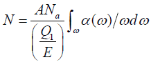 (2)
(2)
where, N-and Avagadro number (Q1/ε) integral unit measuring the strength of the hydride sm2/mol, (Q1/ε)=3,5. If the width of the absorption denoted by Δω and the center frequency ω0, then Δω/ω0 ≤ 0,1, when approximation with an accuracy of ± 2% (2) can be written as follows:
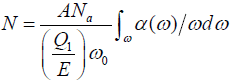 (3)
(3)
Where:
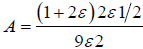 ; ε=the dielectric constant. For Siλ ε=12; Ge ε=16. If equation (3) denotes the expression Integral at first AS and JS=
 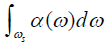 -total absorption stretching modes for each film, then, for determining the concentration of hydrogen (NH), we obtain a general expression in an abbreviated form as:
 (4)
(4)
AS-Factor for film a-Si:H is in the area stretching modes 1,4 · 1020 cm-2. The absorption coefficient (α) for these frequencies (2100 sm-1) is 8·10-1 ÷ 3·102 cm-1 with NH=7·1021 ÷ 2, 1·1022 cm-3. For films of a-Ge:H AS=1,7·1020 cm-2. It is clear that equation (4), as characterized by stretching vibration mode due to the films a-Si: H, a-Ge: H and a-Si1-x Gex: H. Estimates of the relative binding of hydrogen and hydrogenated a-Si1-xGex: H:
 (5)
(5)
Where NSi-H and NGe-H-the concentration of hydrogen in a-Si: H and a-Ge: H (in cm3). Equation (4) can be rewritten for the mode of oscillation (wagging moda) for films with a-Si: H and a-Ge: H. Thus the value of NSi-H and NGe-H are determined from equation (4) for the mode of oscillation in the following form:
 (6)
(6)
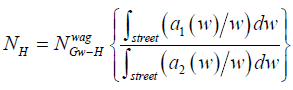
Where,  -modes of oscillation, the total absorption for the films a-Si: H and a-Ge: H. For these films, Aw=1,6 · 1019 sm-2 and Aw=1,1 · 1019 cm-3, respectively. Knowing NGe-H (where, for a film-Ge: H, Aw=1,6·1019 sm-2 and α=5·101 sm-1), calculate the concentration of hydrogen in the film and the NH-Si1-xGex:H by the expression:
 (7)
(7)
Where-the number of links defined by the modes of oscillation in a pure-Ge: H value, which is calculated according to equation (6). The second factor in the expression for NH (integral ratio of IR absorption maxima) is a stretching vibration mode in the sample and a pure-Ge: H. To calculate the integral relation used a maximum corresponding to the stretching vibrational mode Ge-H (2000 cm-1) in the film is a-Si1-xGex:H.
From these data we can estimate the oscillator strength in the film is a-Si1-xGex: H by the relation:
Q=JS/Jw,
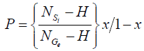
where, 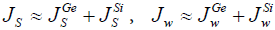 . The quantities are the integral absorption mode of stretching and rocking modes, respectively. Oscillator strength Q=0,51 (for x=0) and Q=0,13 (for x=1). The maximum value of P=4.16 for x=0.40. Table 1 shows the characteristic parameters of amorphous films of a-Si0,60Ge0,40:H. Figure 1 shows the distribution of hydrogen on the film thickness d: 1-by recoil protons, 2 by infrared absorption spectrum. It is seen that the distribution of hydrogen sufficiently uniform. Note that the values of NH, defined by the MOS and IR spectroscopy coincide within 2-3 at %. Figure 2 shows the correlations of concentrations of hydrogen, defined by the effusion of the films. a-Si0,60Ge0,40:H. The concentration of hydrogen (NH), defined by the effusion, correlated to the hydrogen concentration c, calculated using the integrated force Jw, at a frequency of oscillation modes 600 sm-1 (Figure 2). We found that after effusion during heat treatment (350 ÷ 700°C) the concentration of hydrogen CH=1,3÷23,7 at.%. It was found that the oscillator strength f depend on the concentration of hydrogen (CH), they decrease in the effusion of hydrogen with increasing hydrogen content in the atmosphere of the films a-Si0,60Ge0,40:H at partial pressures from 0.6 to 3,0 mTorr oscillator strength increases (Figure 3). This is due to the increase of hydrogen bonds and SiH GeH at the specified frequency. With increasing annealing temperature due Ge-H and Si-H rupture. The concentration of hydrogen films a-Si: H after heat treatment at 350°C and begins to decrease at 700°C is close to almost zero. The shift of the absorption band of the solid relative to the natural frequency of the oscillation modes in the gas is determined from the expression:

Figure 1: Distribute of the hydrogen d- of the layer in the thickness: 1. Proton recoil method, 2. Method of red spectrum of to be swallowing.

Figure 2: a-Si0,60Ge0,40:H correlation of the quantity (amount, number) of the hydrogen specified with effusion method for layers correlation dependence.
When was/were
Layers, pressure of the hydrogen at = PH2 0,6 mTorr.
Layers, pressure of the hydrogen at = PH2 1,2 mTorr.
Layers, pressure of the hydrogen at = PH2 1,8 mTorr.
Layers, pressure of the hydrogen at = PH2 2,4 mTorr.
Layers, pressure of the hydrogen at = PH2 3,0 mTorr.

Figure 3: The dependence of the hydrogen partial pressure (PH2) (line 1) and the concentration of hydrogen (CH) (curve 2) of the oscillator strength (T) in amorphous films of the solid solution a-Si0,60Ge0,40:H.
| № layer | PH2 mTоrr | E0 eV | P | CH at% | NSi:H cm-3 | NGe:H cm-3 | NH cm-3 | IS(Si) | IS(Ge) | IW(Ge), IW(Si) | IS/IW |
|---|---|---|---|---|---|---|---|---|---|---|---|
| 1 | 0,6 | 1,32 | 1,85 | 1,3 | 6,2·1021 | 2,2·1021 | 3,1·1020 | 7,2·101 | 6,3·101 | 6,0·102 | 0,13 |
| 2 | 1,2 | 1,36 | 2,29 | 5,1 | 9,4·1021 | 2,7·1021 | 4,0·1021 | 8,6·101 | 7,5·101 | 5,2·102 | 0,18 |
| 3 | 1,8 | 1,41 | 2,59 | 8,7 | 1,3·1022 | 3,3·1021 | 5,1·1021 | 9,4·101 | 8,3·101 | 4,0·102 | 0,26 |
| 4 | 2,4 | 1,44 | 3,38 | 14,7 | 2,1·1022 | 4,1·1021 | 6,2·1021 | 1,0·102 | 9,0·101 | 3,0·102 | 0,38 |
| 5 | 3,0 | 1,52 | 4,16 | 23,7 | 2,9·1022 | 4,6·1021 | 9,7·1021 | 1,1·102 | 1,0·102 | 2,7·102 | 0,51 |
Table 1: Characteristic parameters of the amorphous layers a-Si0,60 Ge0,40:H.
 (8)
(8)
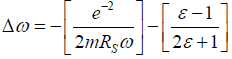
Where, e* is the effective charge, m-reduced mass of the dipole, R-radius of the sphere volume, in which the dipole; ε-dielectric constant of the matrix. The quantity e* is determined from the relation:
 (9)
(9)
Δω=20 cm-1. The resulting theoretical values coincide with the experimental data.
Optical properties of films from the hν dependence  allow to determine the width of the band gap for each film. In all the studied films of the coefficient of the optical absorption edge is described by the relation:
 (10)
(10)
Where, α=5·104 ÷105 cm-1, E0-optical band gap for each film, B-coefficient of proportionality. The value of B is determined by extrapolating depending on hν for each sample. The quadratic dependence (10) obtained theoretically for a model of Tauc, which describes the density of states of the mobility gap. The value of B at x=0 ÷ 1 is from 527 to 343 eV-1, sm1/2, respectively, E0=1,14 ÷ 1,86 eV for films with a-Si1-xGex:H (x=0 ÷ 1).
EPR-spectra of amorphous films of a-Si1-xGex:H
The EPR spectra of the films a-Si1-xGex:H shooting at 80 K on the RE-1316 spectrometer with a working frequency of 9,4 GHz (B=3.2 cm). The spectra have an asymmetric shape, as composed of two species belonging to the free links of Si and Ge, respectively. However, the observed signal is not a simple superposition of the signals for Si and Ge, as they interact strongly with each other and the resulting in an intermediate range of aims accepted form of a single line. Therefore, the observed spectra on the left and right can be described by a superposition of these two signals: a factor of g=2,018-2,022 and a line width of 73-86 G and g=2,004-2,006 and the line width 51-65 G, respectively, related to the silicon and germanium dangling bonds [10].
For films of a-Si1-xGex:H value of g depends on x decreases, respectively, of 2.005 and 2.018 to 2.003, i.e, the values for the free bonds of silicon and germanium to the corresponding values for carbon. In other words, in the systems Si-Ge, the values of g-links to free silicon or germanium are reduced [10]. In Figure 4 shows the characteristic shape of the EPR line in the films a-Si1-xGex:H (where x=0.20). g-factor was determined by double integration of the differential curves. Bringing to the overall scale was performed using a standard MgO:Mn2+.

Figure 4: The characteristic shape of the EPR lines, taken at 80 K: (а) a-Si1-xGex:H, where х=0,4 and H=21 ат. %, g=2,006, (б) a-Si:H before annealing g=2,005, after annealing at 550°C g=2,003; (в) a-Ge:H before annealing g=2,018, after annealing at 550°C g=2,003.
Electric and photoelectric properties of the films a-Si1-xGex:H, Measurement of the dark conductivity of the film shows that it can be represented as the sum of two components, high-temperature (above T ≥ 200 K) and low temperature (below T ≤ 200 K):
 (11)
(11)
Films a-Si1-xGex:H, ΔE-(x=0 ÷ 1) varies in the range 0,5 ÷ 1,0 eV. Dependence on x for films a-Si1-xGex:H, (at 500 ≥ T ≥ 200 K) the localization of α-1=7 ÷ 10 Å, density of states N (EF)=1016 ÷ 1018 cm-3 eV-1. The energy jumps E=0,012 ÷ 0,091 eV, the hopping length R=70÷150 Å.
Figure 5 shows the dependence of the band gap of the activation energy of electrical conductivity of the films a-Si1-xGex: H, where x=1 (1), 0.75 (2), 0.6 (3), 0.5 (4), 0.4 (5) 0.3 (6), 0.1 (7) 0 (8). Pre-exponential factors vary within the σ01=10-3 ÷ 5·101 ohm/cm and σ02=10-7 ÷ 10-4 Om/ sm. When added to a film-Si:H 40 at % Ge mobility of electrons and holes, the band gap, photoconductivity, recombination lifetime and the activation energy of electrical conductivity is greatly reduced (Figure 6). In the weak absorption A=1 and γ=0,4 ÷ 0,9. The results obtained show that the parameter γ depends on the concentration of atoms Ge and not on other parameters in the films as-Si: H (Figure 6), for example, the substrate temperature and film thickness.

Figure 5: The dependence of the band gap of the activation energy of photoconductivity for films a-Si1-xGex: N. Curves: 1–х=1; 2–х=0,75; 3–х=0,60; 4–х=0,50; 5–х=0,40; 6–х=0,30; 7–х=0,2; 8–х=0.

Figure 6: Dependence of the photoconductivity γ on the concentration of silicon for a-Si1-хGeх:H (where, х=0 ÷ 1). Notation is the same as in Figure 5.
Creating a solar cell
Studies show that a film Si1-xGex: H (x ≥ 0, 20) can be used as highquality material in the semiconductor electronics. For this purpose we have developed a three-layered element based on two-layer cascadetype elements. Three-layer element is made of double-layer element, which consists of two elements based on a-Si: H pin junction and a pin element with i-layer film of a-Si0,88Ge0,12:H (Figure 7). Thickness of the i-layers for the top two hits were selected in such a way as to meet the condition of equality of the short circuit current of the lower element. Short-circuit current was about half the value for a single pin junction. Open-circuit voltage increases and short-circuit current decreases with an increase in the number of superimposed layers. This method can increase the number of layers (a n-layer cell). Note that for each element were made i-layer thickness of 0.5 microns. The area of each element was 1.3 cm2. When you receive a three-layer solar cells must be maintained uniform thickness and size for each item. Substrate material was selected steel and as a coating used Z2O2 with transmission of light of 80%. ZrO2 coating simultaneously plays the role of the upper (front) contact (Figure 8). The thickness of the layers of a-Si: H p-and n-type was ~ 300 and 400 Å, respectively.

Figure 7: Dependence of the photoconductivity νμDτ, σф, σf, the drift mobility of holes (μр) and electrons (μn) of the atom. % Ge films for a-Si1-хGeх:H (где х=0 ÷ 1). Deposition conditions are shown in Figure 5.

Figure 8: Structure diagram of a three-layer element in which i-layer is made on the basis of a-Si0,88Ge0,12:H.
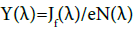
Doping level consistent with [B2H6/(SiH4+GeH4)] ≤ 10-4 for the p-type films and [PH3/(SiH4+GeH4)] ≤ 10-4 for n-type films. B2P6 and the number of PH3 has changed in the range 0,1 ÷ 0,5% with the ratio of gas mixtures. After the deposition of amorphous semiconductor layers deposited by evaporation of ZrO2 film thickness of ~ 500 Å. The upper contacts using Ni/Ag, for the lower-stainless steel substrate. Elements of sunlight illuminated the source of the AM-1 (100 mVt/sm2). Short circuit current for three-layer elements was 8.5 mA/cm2, open circuit voltage of ~ 2.25 V, fill factor of ~ 0.50 and η (efficiency)=9.5% (Figure 9). Similarly, the efficiency for single element is 7% and double-layer element of 8.9%. Figure 10 shows the collection efficiency for single, two and three elements of the wavelength of light at a flux of photons 1016 ÷ 1018 fot./m2c in the short-circuit mode. Collection efficiency of carriers at different wavelengths is defined as:

Figure 9: (a) The dependence of the optical absorption coefficient α on the photon energy hν films a-Si1-xSh: H (x=0 ÷ 1) doped with phosphorus; (b) Dependence (αћν) 1/2 of the energy of the photon (ћν) films a- Si1-xSh: H (x=0 ÷ 0,32). (1) x=0; (2) x=0.06; (3) x=0.17; (4) x=0.25; (5) x=0.32. Terms modes are described in the text.

Figure 10: The dependence of the collection efficiency of the wavelength of the incident radiation: (1) Cascade solar cell UN/a-Si: H (2) Cascade solar cell a-Si1-xCx: H/a-Si: H (3) The solar cell type Schottky barrier.
 (12)
(12)
Where Jf(λ)-photocurrent density (10 mA/cm2), N(λ)-the number of photons incident per unit area per second, e-charge of free carriers (Figure 11). To increase the η for the solar cell is required to increase the number of layers, to reduce the area of the elements, the choice of metal wires, to reduce the resistance of metallic contacts, etc.

Figure 11: Spectral characteristic double-barrier structure after irradiation with gamma rays: (1) Up irradiation, (2) Dose 150 krad (3) Dose of 200 krad (3') Annealed at T=450° C for 30 min.
Conclusion
Plasma-chemical deposition method using gas mixtures of H2+SiH4; H2+GeH4 in various proportions were obtained thin films of a-Si1-xGex: H (x=0 ÷ 1). It is shown that the absorption coefficient for visible light and the band gap increases with increasing silicon content. The mobility of carriers and photoconductivity decreases sharply when the content of germanium more than 40 at % In the film as well-Si: H. On the basis of a film-Si:H and a-Si0,88Ge0,12:H solar cells are made and created single-layer, dual-layer and three-layer structure, measured their characteristics. We found that the area of 1.3 cm2 element η of 7%, 8.9%, 9.5%, respectively. For the three-layer element maximums collection efficiency shift toward longer wavelengths. In the structures obtained in the wavelength range 0,3 ÷ 1,1 mm up to 120 h of degradation was not observed. It is shown that the structure of solar cells based on a-Si0,88Ge0,12:H and a-Si:H are effective and further work to improve the quality of the films and increase their efficiency is an urgent task.
References
- Bakaleynikov LA, Flegontova EJ, Pogrebitsky K, Eremin IV (2004) Theoretical principles of semiconductor detector based on the p-n junction. Technical Physics 9: 74.
- Kosyachenko LA, Maslyanchuk EL, Rarenko IM, Sklyarchuk VM (2004) Issledoanie carrier collection CdZnTe-ray detectors and radiation photoelectrically. Semiconductors 388: 1018.
- Madatov RS, Mehrabova MA, Abasov FP (2006) Fast acting detectors for g-quantums on the Au-Si. The IV Euroasian Conference on Nuclear Science and its Application, Baku, Azerbaijan.
- Madatov RS, Abasov FP, Mustafayev Yu M (2011) Effect of Gamma irradiation on the photoelectric parameters of a two-barrier structure based on silicon. Russian Conference on Semiconductor Problems, Novosibirsk.
- Abasov FP (2014) Production of thin films for the creation of solar cells. Photonika 2:72-90.
- Abasov FP (2014) Influence of Gamma radiation on electrik propertien of silicon solar cells. Int J Pure Appl Sci Technol 21: 12-16.
- Abasov FP (2014) Effect of Gamma irradiation on electrophysical and photoelectric parameters of double-barrier structure based on silicon. Nuclear Science and its Application. Vll Eurasian Conference, Baku.
- Abasov FP (2016) Effect of Gamma irradiation on photoelectric parameters of double-barrier structure based on silicon. J Material Sci Eng 5: 269.
- Abasov FP (2016) Study of radiation effects on photoelectric and luminescence parameters of two-barrier structures based on silicon. 2nd International Conference on Condensed Matter Physics, Chicago, USA.
- Abasov FP (2016) Determining the amount of hydrogen in thin films well for solar cells. Int J Sci Res Eng 1: 1-14.
- Abasov FP (2016) Determining the amount of hydrogen in thin films well Si1-Xgex_ H (X = 0 · 1) for electronic devices. J Material Sci Eng.
Citation: Abasov FP (2018) Effect of Qamma Irradiation on Optoelectronic Properties of Two Barrier Structures of Nano Crystalline Silicon Solar Cells. Innov Ener Res 7: 181. DOI: 10.4172/2576-1463.1000181
Copyright: © 2018 Abasov FP. This is an open-access article distributed under the terms of the Creative Commons Attribution License, which permits unrestricted use, distribution, and reproduction in any medium, provided the original author and source are credited.
Select your language of interest to view the total content in your interested language
Share This Article
Recommended Journals
Open Access Journals
Article Tools
Article Usage
- Total views: 4406
- [From(publication date): 0-2018 - Nov 07, 2025]
- Breakdown by view type
- HTML page views: 3518
- PDF downloads: 888