Research Article Open Access
Biomedical Signal Processing through Wireless System for Body Sensor Networks
Deepak Choudhary1* and Umesh Sehgal21Associate Prof, ECE Department, Galgotia’s University, India
2Associate Prof, CSE Department, Arni University, India
- *Corresponding Author:
- Dr. Deepak Choudhary
Associate Prof, ECE Department, Galgotia’s University, India
E-mail: engg_deepak@yahoo.com
Visit for more related articles at International Journal of Advance Innovations, Thoughts & Ideas
Abstract
Recent years have seen the rapid development of biosensor technology, system-on-chip design and wireless technology and ubiquitous computing. When assembled into an autonomous body sensor network (BSN), the technologies become powerful tools in wellbeing monitoring, medical diagnostics, and personal connectivity. In this paper, we describe the first demonstration of a fully customized mixed-signal silicon chip that has most of the attributes required for use in a wearable or implantable BSN. Our intellectual-property blocks include low-power analog sensor interface for temperature and pH, a data multiplexing and conversion module, a digital platform based around microcontroller, data encoding for spread-spectrum wireless transmission, and a RF section requiring very few off-chip components. The chip has been fully evaluated and tested by connection to external sensors, and it satisfied typical system requirements.
Keywords
Body sensor networks, low-power biomedical circuits and systems, microsystems, system-on-chip (SOC).
Introduction
The ability to integrate complete sensor systems into a very small form factor is of growing importance as applications such as ubiquitous computing [1], micro total-analytical-systems (TAS) [2], wearable electronics [3], and body sensor networks (BSN) [4], [5] become more widespread. One of the earliest examples of these technologies was demonstrated by Mackay in 1961 [6]. An important aspect of Mackay’s work was that his device was made possible by the then relatively recent invention of the transistor. More recent developments have sought to make use of recent technological developments. Examples are the development of Smart dust that uses microelectromechanical systems technology to explore the extremes of miniaturization [7], micro-robotics for gastrointestinal investigation [8] and other sophisticated BSNs using discrete electronics components-based devices [9]. Quite often, the relative large size of these devices significant limits the performances as well as the pervasive deployments.
In this paper, we describe the development of a wireless biomedical sensor interface system-onchip (SOC) that aims to combine many of the functions of the BSN micro-systems onto a single substrate. Our design is specified for a biosensor system with up to eight pH and temperature data channels communicating via an encoded wireless interface to a remote base station. The system comprises analog sensor interface circuit, data-conversion circuits, a microcontroller, a data encoder, and a frequency-shift keying (FSK) RF transmitter. Many of the system blocks were imported in an intellectual-property (IP) block form; thus, the design represents the first steps toward a generic BSN-on-chip [10].
Wireless Sensor Interface System On Chip
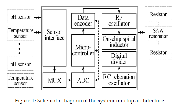
Fig. 1 shows the complete system diagram of the SOC we have developed. The design flows used to create the SOC was relatively straightforward. Cadence tools were used for analog/digital simulations and back-end design tasks and Synopsys tools were used for digital synthesis of VHDL/Verilog behavioral and register transfer-level descriptions. Transistor-level and gate level simulations were used to verify that all functional blocks worked as desired before chip assembly and implementation. The microcontroller block was verified by writing to a XILINX SPARTANIIFPGA, followed by board-level testing to ensure proper functionality before committing to silicon (Si) [11].
Sensor Interfaces
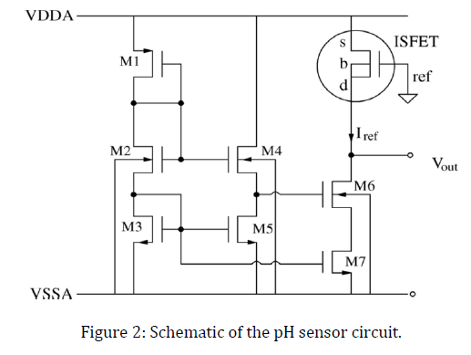
The SOC operates with external pH (acidity/alkalinity) and temperature sensors. The pH sensor used here is an ion-sensitive field-effect transistor (ISFET) and has a Nernstian response with respect to pH [4]. Unfortunately, this device also has a response to temperature change that must be calibrated for. As a consequence, the temperature sensor is not only required to provide a temperature reading per se, but is also required to enable calibration of the pH sensor. The external temperature sensor is a forward biased pn-junction with a junction area of 0.6 mm. The interface circuit is a conventional structure that connects the diode in feedback across an operational amplifier with a constant bias current. An on-chip bias resistor sets the constant current to be approximately 15A. The reverse bias saturation current of the diode is 30 pA and the ideality factor is approximately 2; therefore, the device sensitivity 22 C, but does vary from device to device due to tolerances. The external pH-ISFET sensor forms the load of a 33- A cascade current sink as shown in Fig. 2. The ISFET is similar to a MOSFET device where the gate metal was replaced by a reference electrode immersed. The ISFET has an intrinsic gate referred sensitivity of a 43-mV/pH point. For circuit implementation, the cascade structure of the current source allowed a high impedance to be obtained, which reduced the variations of the drain-source current due to the fabrication, temperature, and power-supply variations. The output transistors of the cascade circuit form an active load to the ISFET that is configured as a source follower; thus, the voltage swing at the source of the ISFET responds at the 43- mV/pH point.
Mixed-Signal System Platform
The analog-to-digital interface circuitry comprises seven 2-input multiplexers and a 10-b successive approximation analog-to-digital converter (ADC). Power supplies were directly connected as the reference voltages of the ADC. The microcontroller-driven multiplexers allow eight sensor channels to be presented to a single ADC for 0.3 ms each, hence, 2.4 ms is required to sample all eight channels. However, the system sample rate was set to be approximately 0.5 S/s, by which we mean all eight channels are sampled once every 2 s. In order to minimize the off chip component count, hence, the overall packaged system size, we used an on-chip RC relaxation oscillator to generate the input to the chip timer circuit.
The first-order relaxation oscillator was based on charging or discharging an on-chip timing capacitor via a precision current source, which provided a cost-effective solution as well as design simplicity and programmable ability. The oscillation frequency of the relaxation oscillator was proportional to the value of the charging current and was inversely proportional to the value of the timing capacitor. The relaxation oscillator circuit was designated with an operational transconductance amplifier, a comparator, an inverter, the sampling switches and capacitor, and a controlled current source. The relaxation oscillator has an automatic swing control loop to rectify the oscillation amplitude adaptively in order to provide symmetrical oscillation waveforms.
The timing precision of the oscillator is poor due to the fabrication tolerance of on-chip resistors and capacitors, but this imprecision is not important in the context of the complete system [13]. The nominal frequency of the RC oscillator is set to be 8 MHz, but it measures only 7.1 0.1 MHz on a batch of ten fabricated chips. The timer circuit contains a digital divider designed to generate different clocks for the ADC (250 kHz), the microcontroller (250 kHz), and the data encoder (32 kHz). The clock rates for these blocks are 224 kHz, 224 kHz, and 29 kHz, respectively because of the shift of the nominal oscillator frequency. The timer can generate the originally intended clock frequencies when it is connected to an oscillator implemented in the RF section of the SOC, but this requires an additional off-chip surface-acoustic-wave (SAW) resonator and two resistors. However, in order to save power, the RF oscillator is not used for timing, but only when wireless transmission is required (see Section II-C). In addition to generating the system clocks, the timer also generates a positive pulse (lasting 5 s) every two seconds to start the microcontroller.
The microcontroller was designed by us to have the identical instruction set, excluding the multiply (MUL) and WAIT instructions, as a Motorola 6805 CPU. The microcontroller was designed to be fully static and was implemented with 512-B ROM, 32-B RAM (24 B for buffers and 8 B for stack), three bidirectional 8-b input/output (I/O) ports and a 16-b capture/compare timer system. The software routines, embedded into the 512-B ROM, were used for scheduling different tasks, such as channel cycling, data sampling and packet forming, and automatically go into a sleep mode when all tasks are finished. However, every two seconds, the aforementioned positive pulse generated by the timer invokes a rising-level sensitive interrupt of the microcontroller, and forces the microcontroller to go back to an active mode. This external interrupt design enables dynamic re-configuration of the system sample rate [14]. For example, by simply setting different time intervals between the positive pulses, the microcontroller can be invoked at varying time intervals in order to suit different applications and data needs. All output data are represented as a serial bit-stream packet by the microcontroller. One packet has two identical data episodes with a total of 192 information bits. Each episode begins with eight start bits with a well-defined signature, eight channels (8-b each) of physiological data plus an even parity bit, two 8-b buffer contents (for ID and future expansion) and an 8-b stop sequence. There are 64 ‘0’ b between two consecutive packets. The microcontroller was programmed for the duration of representing each bit to be 7.81ms. In practice, it takes 8.7 ms to represent each bit because of the shift of the clock rate from 8 MHz to 7.1MHz. Therefore, the microcontroller’s serial port data rate is approximately 115b/s. The bit stream signal from the microcontroller is fed into a programmable transmitter for wireless transmission.
Wireless Interface
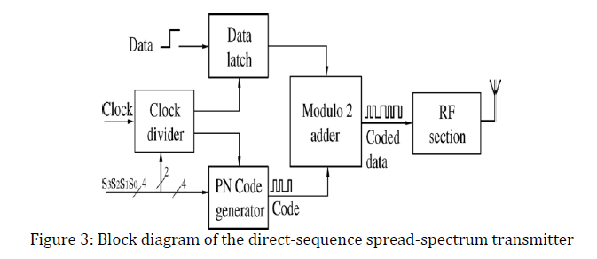
In order to improve the wireless transmission reliability, a programmable direct-sequence spread-spectrum (DS-SS) transmitter is integrated into the SOC with very few off-chip components [5]. The transmitter comprises a data encoder and RF-section. A block diagram of the transmitter is shown in Figure 3. The multiplication process is a simple modulo-2 adder that also acts as a phase modulator. The core of the DS-SS transmitter is the pseudorandom noise (PN) code generator [6]. The PN code generator consists of an eight-stage linear feedback shift register (LFSR) and a multiplexer. The PN code length was programmable to provide the appropriate amount of data spreading for a particular application. The transmitter also comprises a memory block for storage of data. In the LFSR implementation, the all 0 state (all 1 state if XNOR is used in the feedback path) is not allowed. In the design, this was prevented by an additional control circuit. This rearrangement also enables the generation of even length PN codes by inserting an additional 0 to give a maximal LFSR sequence. Serial bit-stream data to be transmitted are coded by either the PN code if the bit is logic 0 or a 180 phase-shifted version of the PN code if the bit is logic 1. This coding is performed automatically by the EXOR operation. For a PN code length of 256, 128, 64, and 32 b, it takes approximately 34 s, 68 s, 136 s, and 273 s, respectively, to present one code. The minimum data rate from the encoder is approximately 3.67 kb/s, which is 32 times the microcontroller’s serial port data rate (115b/s).
The integrated RF section on the SOC could be activated. The amplification stage of the RF session was elaborated to be a near-class-E RF power amplifier that was driven by the encoder’s digital output. A two-stage driving amplifier was utilized. The gain budget of this amplifier was carefully asserted to maintain high gain and linearity while limiting the total current. The amount of amplitude and bandwidth extensions was optimized for this design in order to minimize data jitter. In the output stage, the back-termination poly-silicon resistors were used to reduce reflections from output ports. A relatively low carrier frequency was selected for the on-chip RF section. This is because, applications, such as the implantable laboratory-in-a-pill in-situ experiments, have confirmed that low-frequency signals are less strongly absorbed [7], [8] and regulatory requirements allocated for 30MHz. The carrier frequency signal was generated directly by using an oscillator with an external SAW resonator, rather than by having a low-frequency oscillator multiplied up to the desired frequency. For exploratory purposes, the RF section had two resonator controlled oscillators, each with a frequency-shift keying (FSK) modulator and an output stage. One was a Pierce circuit and the other was a Colpitts oscillator. The circuits’ satisfied the Barkhausen criterion with closed-loop gain1 and the phase shift of the signal from the input to the output of the amplifier was 180. To achieve low phase noise, only one active transistor was used in the core circuits. Negative resistance was created by using the RF-NMOS transistor in the common source configuration for the Pierce oscillator and the common gate configuration for Colpitts oscillator. The SAW resonator was used as a frequency determination element between the drain and the gate of the NMOS transistor for the Pierce oscillator, and the source and the gate for Colpitts oscillator, respectively. A variable capacitor in series with the SAW resonator was used to generate FSK modulation. The main advantage of using the SAW resonator was relatively high quality factor and relative low power consumptions. Test results showed that the Colpitts oscillator consumed less power (5.1 mW at 3.0 V) than the Pierce oscillator (8.1 mW at 3.0 V). An on-chip spiral inductor (approximately 800μm X 300μm) incorporated on the SOC can be used. The radiated signal from the inductor was detectable at a range of 0.5 m in air using a Win radio receiver with a conventional whip antenna at a data rate of up to 5 kb/s. Therefore, the encoder data rate is always set to be 3.67 kb/s. Tests indicated that the on-chip inductor was less efficient than an external antenna; however, it demonstrated the possibility of integrated antennas on silicon [2].
The signal from the SOC is detected by a data-acquisition (DAQ) device. Since the DAQ terminal uses a correlator implemented on a PC in software, the synchronization requirement between the SOC and the terminal was significantly reduced. The correlator will yield a positive peak at 0 phases and a negative peak at 180 phases. Data can be simply recovered by thresholding the correlator output. Fig. 4 shows an experimentally obtained decoded signal after normalized autocorrelation, with the on-chip RF section activated. It shows that different bit values (1 or 0) were correctly recognized despite the noisy background introduced by the wireless interfaces. We conclude that the programmable transmitter provided an adequate wireless interface in a noisy environment by rejecting narrowband interference.
Chip Assembly
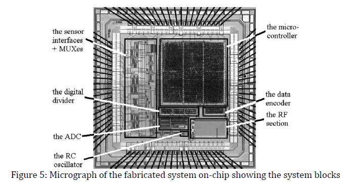
The sensor interfaces, the system platform, and the wireless interface were implemented on a 4.1 mm 4.1-mm mixed signal SOC prototype, including a second ring of m pads, added to ease manual bonding in micro-system prototypes. The chip was fabricated using a three-metal, 2-poly 0.6- m CMOS process provided by the AMS. Finished chips were returned as unpackaged die (Fig. 5) and in 84-pin J-leaded ceramic chip carrier (JLCC) packages for test purposes. Table I indicates the number of gates and silicon area corresponding to individual circuit blocks. The size of the SOC prototype, excluding the second pad ring, is core limited, its core occupying a total of 6.3 mm of silicon area. Of the 84 pads, 24 are power pads and 60 are input/output (I/O) pads, more than 75% of which are used for the preliminary chip test.
The design of a multifunctional SOC creates many problems due to individual components contributing to the overall noise budget. Previous designs [6] have shown that the limiting factor on noise is on-chip substrate noise due to clock transmission rather than thermal or shot-noise sources in the sensor architecture. We have therefore given great consideration to chip-assembly and routing in order to minimize on-chip coupling as far as possible using conventional layout techniques.
The SOC was designed to minimize the propagation of noise from the noisy 40-MHz RF oscillator (with the on-chip RF oscillator activated) to the noise-sensitive sensor interface circuitry, and particularly to the operational amplifier input nodes. These circuits were physically isolated on the silicon die, their power supplies were separated inside the chip, and additional substrate noise barriers (guard rings) were placed around them. More-over, the core and pad ring power supplies were also separated inside the chip, and the pad ring was split into analog, digital, and RF sections to inhibit noise from propagating through the power lines. Finally, approximately 20 pF of powersupply decoupling capacitance was distributed between different rails (i.e., RF ground and analog ground [11].
Testing of the SOC revealed that the biggest contributor of noise that reaches the analog amplifier inputs is the resonator- controlled oscillator within the RF section. It generates 15 Mv and 25 mV of noise at 20 MHz and 40 MHz, respectively, as measured at the operational amplifier input nodes. The on-chip RC oscillator operating at 7.1 MHz generates 13 mV of noise as measured at the operational amplifier input nodes and produces lower peak-to-peak noise in the same measurement configuration. The total noise measured on an output pin from the analog circuit [before the analogto- digital converter (ADC)] of the SOC, when powered by two batteries, is equal to 15 mVrms.
System Performance
In addition to evaluating each individual block, we have tested the performance of the complete integrated system. A complete functional flows of the SOC, from sensors to a DAQ device, was demonstrated.
Power Consumption
A printed-circuit board (PCB) was used for SOC testing. The packaged SOC was plugged into the PCB and powered by two SR44 silver-oxide cells attached using short leads. The battery voltage decreases with use and the average current consumption of the SOC for different battery voltages is measured. The largest power consumption is from the sensor interfaces and RF sections, which are 1.9 mA at 3 V and 1.7 mA at 3 V, respectively. With the on-chip RF section activated, the maximum measured power consumption for new batteries was 18 mW, decaying to 8 mW for batteries approaching the end of their life-time. No significant perform deteriorations were affected by decreasing battery levels within the battery operation ranges.
Functionality
To demonstrate the functionality of the sensor interfaces and the system platform, a temperature sensor and a pH sensor (as described in Section II-A) were connected to the sensor interface circuitry. The binary output signal from the microcontroller’s serial port was fed into a DAQ package (National Instruments DaqPad-6020E) with a wired setup. A laptop computer with appropriate software was configured for use as the DAQ and data presentation terminal. A data-processing algorithm using oversampling was developed in MATLAB and used to recover the raw sensor information [12]. The oversampling rate was 1 kS/s (the microcontroller’s data rate is 115b/s). For calibration purposes, the sensors were first dipped into specified pH buffer solutions at known temperatures in the range 30 to 90 C. Once calibrated, approximately 25 min of data were acquired for each experimental run. Readings from standard temperature and pH meters were simultaneously recorded for comparison. From this study, we were able to confirm that the sensor interfaces and the system platform were working together as described in Sections II-A and B.
Finally, the SOC, consisting of the sensor interface, the system platform, and the complete wireless interface was tested. The output of the digital encoder was fed into the on-chip RF section using an external SAW resonator to tune the transmitter. The data-processing algorithm at the receiver was updated to use the correlation computations described in Section II-C to accommodate the new signal. The PN code was selected to give the lowest data transmission rate of 3.67 kb/s. The oversampling rate of the DAQ device was set to be 10 kS/s in order to correctly sample the signal. The same scan receiver was used for continuity. In-vitro results indicate the complete SOC works as intended. The results are comparable with those obtained by using the external TX module.
Conclusion
We have presented a fully specified and functional biomedical sensor interface system-on-chip to acquire, process, and communicate sensor data wirelessly. The design represents a prospective BSNon- chip framework using IP blocks that we have developed by ourselves. The intellectual-property blocks include the analog sensor instrumentation for temperature and pH, a data multiplexing and conversion module, a digital platform based around an 8-b microcontroller, data encoding for spread-spectrum wireless transmission, and an RF section requiring very few off-chip components. We believe that the concept we present here can be greatly developed to introduce sensor-SOC into a diverse range of BSN applications.
References
- N. Davs and H. W. Gelle , “Beyond prototypes: Challenges in deploying ubiquitous systems,” IEEE Pervasive Comput., vol. 1, no. 1,pp. 26–35, 2006.
- O. P. Naji, P. B. Monaghan, and A. Manz, “Can microTAS be alternatives for sensors?,” in Proc. IEEE Sensors, 2006, pp.680–683.
- G. Iddan, G. Meron, A. Glukhovsky, and P. Swain, “Wireless capsule endoscopy,” Nature, pp. 405–417, 2007.
- R. S. Mackay, “Radio telemetering from within the body,” Science, vol.134, pp. 1196–1202, 1961.
- B. Warneke, M. D. Scott, B. Liebowitz, L. Zhou, C. L. Bellew, J. A.Chediak, J. M. Kahn, B. E. Boser, and J. Pister, “An autonomous 16 mm3 solar-powered node for distributed wireless sensor networks,” in Proc. IEEE Sensor, 2005, pp. 1510–1515.
- H. J. Park, H. W. Nam, B. S. Song, J. L. Choi, H. C. Choi, J. C. Park,M. N. Kim, J. T. Lee, and J. H. Cho, “Design of bi-directional and multi-channel miniaturized telemetry module for wireless endoscopy, in Proc. IEEE-EMBS Special Topic Conference on Micro Technologies in Medicine & Biology, Madison, WI, 2006, pp. 273–276.
- M. Mar, B. Sullam, and E. Blom, “An architecture for a configurable mixed-signal device,” IEEE J. Solid-State Circuits, vol. 38, no. 3, pp.564–568, Mar. 2004.
- K. Ma, and Q. Yao, “A software/hardware co-design methodology for embedded microprocessor core design,” IEEE Trans.Consum. Electron., vol. 45, no. 4, pp. 1241–1246, Nov. 1989.
- Reid,J. M. Cooper, and D. R. S. Cumming, “A programmable microsystem using system-onchip for real-time biotelemetry,” IEEE Trans. Biomed.Eng., vol. 52, no. 7, pp. 1251–1260, Jul. 2005.
- N. Aydin, T. Arslan, and D. R. S. Cumming, “A direct-sequence spread-spectrum communication system for integrated sensor micro systems,” IEEE Trans. Inf. Tech. Biomed., vol. 9, no. 1, pp. 4–12,Mar. 2007.
- E. H. Dinan and B. Jabbari, “Spreading codes for direct sequence CDMA and wideband CDMA cellular networks,”IEEE Commun. Mag., vol. 36, no. 9, pp. 48–54, Sep. 1998.
- L. C. Chirwa, P. A. Hammond, S. Roy, and D. R. S. Cumming, “Electromagnetic radiation from ingested sources in the human intestine between 150 MHz and 1.2 GHz,” IEEE Trans. Biomed. Eng., vol. 50, no.4, pp. 484–492, Apr. 2005.
- E. M. Biebl, “Integrated active antennas on silicon,” in Proc. SBMO/ IEEE MTT-S Microwave and Optoelectronics Conf., 1997, vol. 1, pp.279–284.
- J. Kim and Y. Rahmat-Samii, “Implanted antennas inside a human body: Simulations, designs and characterizations,” IEEE Trans. Microw. Theory Tech., vol. 52, no. 8, pt. 2, pp. 1934–1943, Aug.2004.
Relevant Topics
- Advance Techniques in cancer treatments
- Advanced Techniques in Rehabilitation
- Artificial Intelligence
- Blockchain Technology
- Diabetes care
- Digital Transformation
- Innovations & Tends in Pharma
- Innovations in Diagnosis & Treatment
- Innovations in Immunology
- Innovations in Neuroscience
- Innovations in ophthalmology
- Life Science and Brain research
- Machine Learning
- New inventions & Patents
- Quantum Computing
Recommended Journals
Article Tools
Article Usage
- Total views: 15319
- [From(publication date):
January-2013 - Apr 01, 2025] - Breakdown by view type
- HTML page views : 10689
- PDF downloads : 4630


