


 26 / 36

Page 60
Notes:
conferenceseries
.com
Joint Conference
July 17-18, 2017 Chicago, USA
International Conference on
DIAMOND AND CARBON MATERIALS & GRAPHENE AND SEMICONDUCTORS
Volume 6, Issue 6 (Suppl)
J Material Sci Eng, an open access journal
ISSN: 2169-0022
Diamond and Carbon 2017 & Graphene 2017
July 17-18, 2017
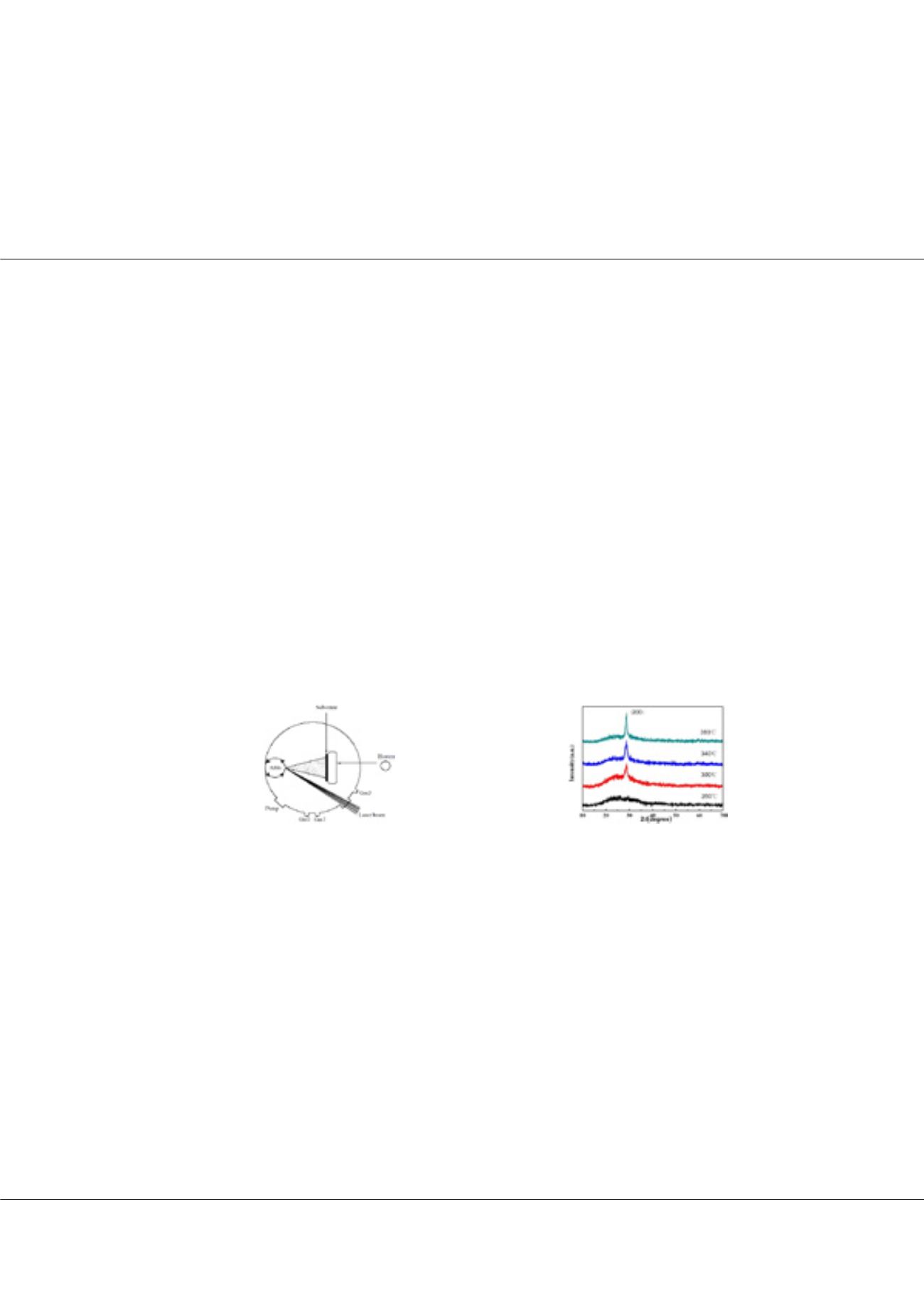
Study onAlSb thin films prepared by pulsed laser deposition
Ping Tang
1,2
, Bing Li
1
and
Lianghuan Feng
1
1
Sichuan University, China
2
Chinese Academy of Sciences, China
A
lSb is a kind of potential absorber material for thin film solar cells. In this paper, AlSb thin films were prepared by using
pulsed laser deposition method, and the effects of substrate temperature on the properties of AlSb thin films were studied.
XRD results showed that the average grain size of AlSb films increased with the increase of substrate temperature. AFM images
suggested that the surface morphology of crystal AlSb thin films was continuous, homogeneous with high compactness. The
electrical measurements showed that the AlSb films were semiconductors with the conductivity activation energy of 0.08,
0.17 and 0.01 eV. At the optimized temperature of 380ºc, the optical band gap of AlSb thin film was 1.52 eV. The obvious
photovoltaic effect has been observed in TCO/ZnS/AlSb/Au device, which demonstrated that AlSb is a potential absorber for
thin film solar cells. In present work, high quality AlSb thin films were prepared by using PLD method and the AlSb thin films
we prepared were used in solar cells. The effects of substrate temperature on the properties of AlSb thin films were studied.
High substrate temperature is helpful for the grain growth of AlSb films. The crystal growth was enhanced and the average
grain size became larger with the increase of substrate temperature. The surface morphology of crystal AlSb thin films is
continuous, homogeneous with high compactness. The electrical measurement exhibits that AlSb thin films prepared by PLD
method are semiconductors with conductivity activation energy of 0.08, 0.17 and 0.01eV. The optical band gap of AlSb thin
film is 1.52 eV at the optimized substrate temperature of 380ºc. Over 30 mV open circuit voltage is obtained in the TCO/ZnS/
AlSb/Au device.
Biography
Ping Tang has her expertise in preparation and characterization of compound semiconductors and photovoltaic devices. Her research interest focuses on the study
of novel compound semiconductors and related solar cells. At present, she is working on the fabrication of AlSb thin films and AlSb/ZnS based solar cells. She has
succeeded in preparing AlSb thin film materials and fabricating AlSb based solar cells with architecture of TCO/ZnS/AlSb/Au and an open-circuit voltage of over
30 mV has been achieved.
ybtangping@163.comPing Tang et al., J Material Sci Eng 2017, 6:6(Suppl)
DOI: 10.4172/2169-0022-C1-076